Wafer Standards
PSL Calibration Wafer Standard, Silica Contamination Wafer Standard
Particle Deposition tools are used to deposit a very accurate PSL size standard or silica particle size standard on the wafer standard to calibrate a variety of wafer inspection systems.
- PSL Calibration Wafer Standard for calibration of wafer inspection systems using a low powered laser to scan wafers.
- Silica Contamination Wafer Standard for calibration of wafer inspection systems using a high powered laser to scan wafers.
Calibration Mask Standard or Silica Mask Standard
Our 2300 XP1 deposits NIST Traceable, Certified mask Standards on borosilicate masks and prime silicon from 75mm to 300mm wafer diameter.
- PSL Calibration Mask Standard on 125mm and 150mm masks
- Silica Contamination Standard on 150mm masks
- 75mm to 300mm Calibration Wafer Standards
- 75mm to 300mm Silica Contamination Wafer Standards
Calibration Wafer Standard – Request a Quote
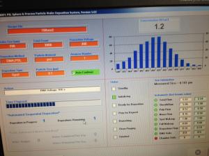
Contamination Wafer Standards, Calibration Wafer Standards and Silica Particle Wafer Standards are produced with a Particle Deposition System, which will first analyze a PSL size peak or silica size peak with a Differential Mobility Analyzer (DMA). A DMA is a highly accurate particle scanning tool, combined with condensation particle counter and computer control to isolate a highly accurate size peak, based on NIST Traceable particle size calibration. Once the size peak is verified, the particle size stream is directed to the prime silicon, wafer standard surface. The particles are counted just before being deposited on the wafer surface, typically as a full deposition across the wafer. Alternatively, up to 8 particle sizes can be deposited as spot depositions at specific locations around the wafer. Wafer standards provide highly accurate, size peaks for size calibration of KLA-Tencor Surfscan SP1, KLA-Tencor Surfscan SP2, KLA-Tencor Surfscan SP3, KLA-Tencor Surfscan SP5, Surfscan SPx, Tencor 6420, Tencor 6220, Tencor 6200, ADE, Hitachi and Topcon SSIS tools and wafer inspection systems.
Applied Physics USA
Differential Mobility Analyzer, DMA Voltage scan, Silica Size Peak, 100nm

Applied Physics USA |
PSL Spheres size standards and silica size standards are scanned by a differential mobility analyzer to determine true size peak. Once the size peak is analyzed, then the wafer standard can be deposited as a full deposition or a spot deposition, or a multiple spot deposition wafer standards. Silica size peak at 100 nano meters (0.1 microns) is scanned above and the DMA detects a true silica size peak at 101nm.
Full Deposition or Spot Deposition Wafer Standards – A particle deposition system provides highly accurate, PSL Calibration Wafer Standards and Silica Contamination Wafer Standards.
Our 2300 XP1 Particle Deposition System provides automatic particle deposition control to produce your PSL Wafer Standards and Silica Wafer Standards.
Particle Deposition Applications
- High resolution, NIST traceable DMA (differential mobility analyzer) sizing and classification exceed the new SEMI Standards M52, M53 and M58 protocol for PSL size accuracy and size distribution width
- Automatic deposition size calibration at 60nm, 100nm, 269nm and 900nm
- Advanced Differential Mobility Analyzer (DMA) technology featuring automatic temperature and pressure compensation for improved system stability and measurement accuracy
- Automatic deposition process provides multiple spot depositions on one wafer
- Full Wafer Depositions across the wafer; or Spot Depositions at any location on the wafer
- High sensitivity permitting PSL sphere and silica particle deposition from 20nm to 2um
- Deposit silica particles for calibration of your wafer inspection systems using high powered laser scanning
- Deposit PSL spheres for calibration of your wafer inspection systems using low powered laser scanning
Deposit PSL spheres and silica particles on prime silicon wafer standards, or your 150mm photo masks.
