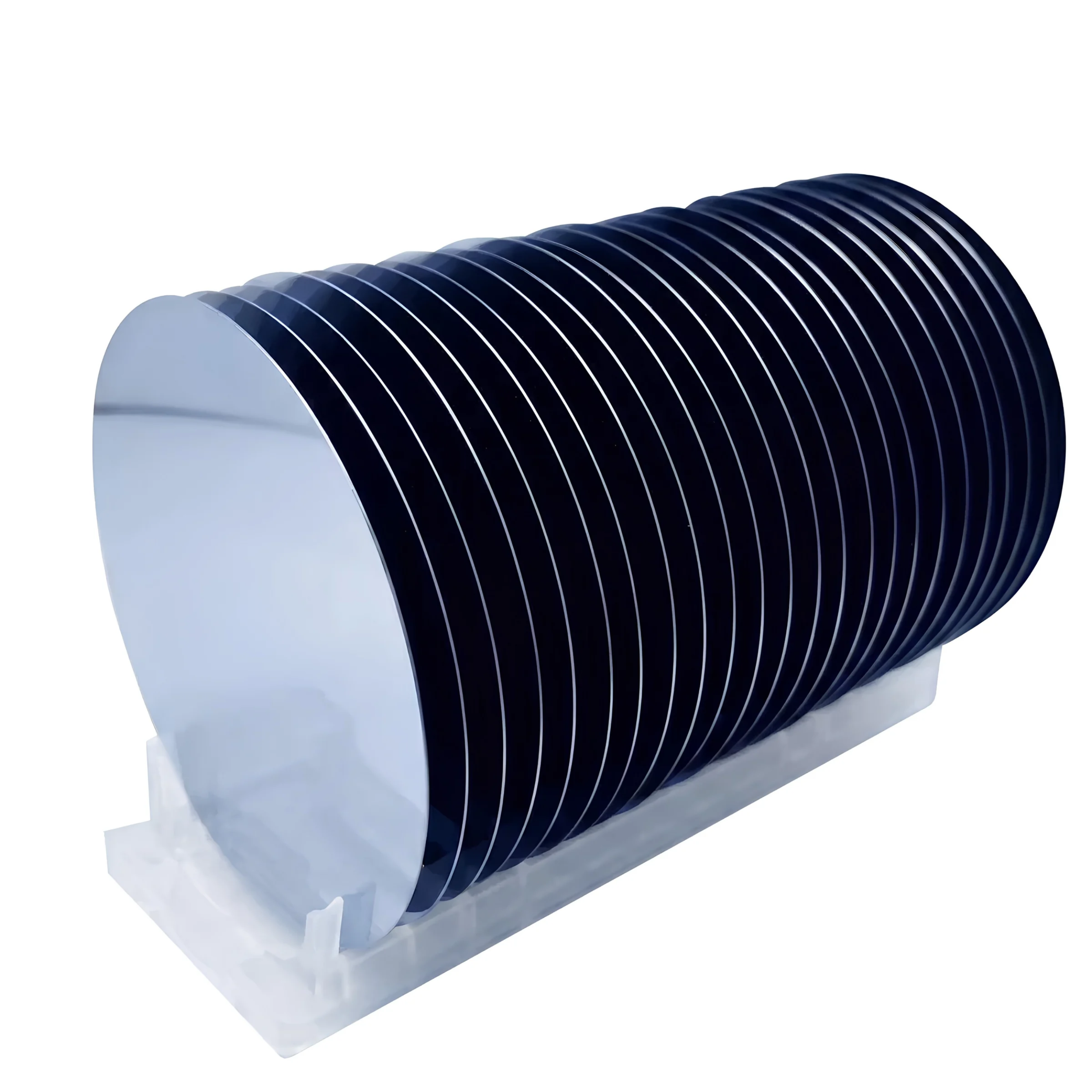
Description
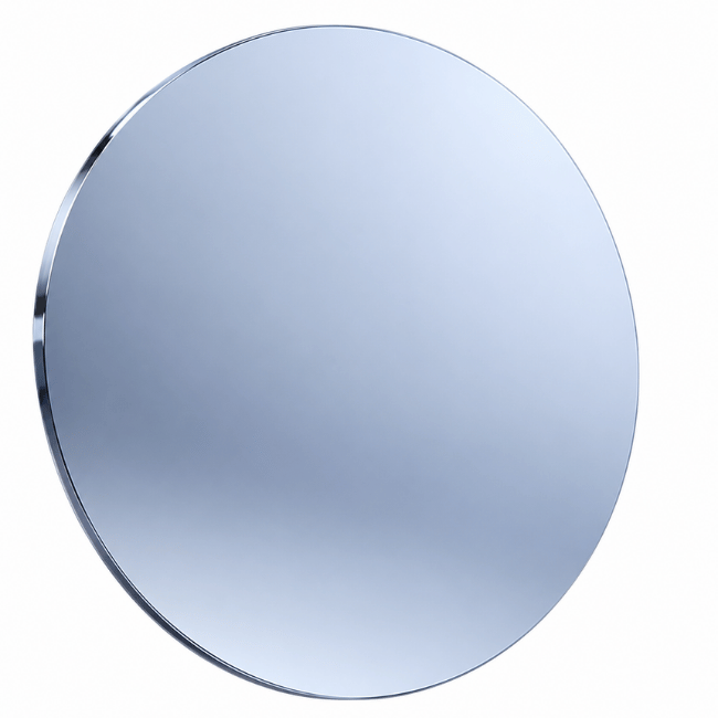
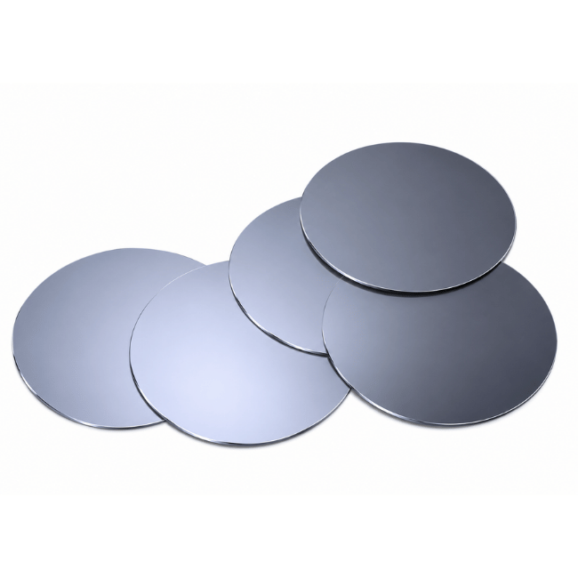
For 125 mm (5-inch) semiconductor operations, maintaining accurate Surface Scanning Inspection Systems (SSIS) is required to prevent yield loss and costly rework. The 125 mm Calibration Wafer Standard provides precise, size-certified particle deposits (PSL or SiO₂) that generate reliable correction curves for your inspection equipment. Designed for long-term stability and compatibility with equivalent SSIS platforms, they are the industry standard for calibrating size responses, running quarterly tool qualifications (Qual-Dep™), and testing chemical cleaning efficiency (PRE).
Deposition Variations:
-
Full Deposit: Features particles deposited across the entire 125 mm surface, essential for verifying the total optical sweep and center-to-edge radial response.
-
1-Spot Deposit: A single-zone deposit with one specific particle size, perfect for targeted single-threshold calibration and quick tool verification.
-
2-Spot Deposit: Delivers two separate sizes in distinct zones, allowing engineers to establish a 2-point sizing calibration curve without needing to swap multiple wafers.