

Applied Physics · Precision technologies since 1992
Request Quote

Semiconductor Metrology & Calibration Standards

ÅP Semiconductor

Semiconductor Metrology & Process Verification

Reference standards, contamination-control tools and electronics-manufacturing systems for teams that need measurement confidence, process repeatability and traceable inspection performance.

Wafer StandardsInspection-tool verification
PSL + SilicaParticle reference materials
SSIS / SurfscanCalibration workflow intent
SMTElectronics production systems
Metrology pathways

Calibration starts with a known reference.

Semiconductor inspection and contamination measurements are only useful when the tool can be challenged against a known standard. Applied Physics supports that workflow with wafer standards, particle standards and related process-verification technologies.

01

Calibration Wafer Standards

Reference wafers with controlled particle deposition for inspection-tool sensitivity and calibration workflows.

  • 75–300 mm wafer sizes
  • Tool sensitivity checks
  • Process/tool matching
Explore calibration wafers
02

Contamination Wafer Standards

Known contamination references for evaluating detection behavior, process monitoring and inspection response.

  • Surface contamination
  • Inspection qualification
  • Process development
Explore contamination wafers
03

Particle Standards

Monodisperse PSL, silica and other particle-reference materials for particle sizing and contamination instrumentation.

  • PSL standards
  • Silica particles
  • Aerosol / liquid applications
Explore microspheres
04

SMT Production

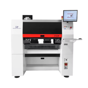
Production equipment for PCB assembly and electronics manufacturing alongside semiconductor process-support workflows.

  • Pick and place
  • Reflow
  • AOI / inspection
Explore AOI systems
Why standards matter

A scanner can be precise and still be wrong.

Surface scanning inspection systems, wafer scanners and particle-detection tools measure contamination at extremely small scales. Optical systems, sensors and calibration references can drift over time.

A known reference standard allows engineers to verify detection sensitivity, particle-size response, tool matching and process stability. That makes the reference standard part of the measurement system—not an accessory to it.

Verify particle-detection sensitivity
Confirm size-response behavior
Match inspection tools across lines
Support acceptance and maintenance checks
Separate process change from measurement drift
Inspection calibration

Built around the questions metrology teams actually ask.

What size should the tool detect? Is the response repeatable? Are two tools seeing the same surface the same way? Is a change in counts process-related or instrument-related?

Wafer-based references

Calibration and contamination wafer standards provide a physical surface reference for inspection-tool qualification, sensitivity checks and process development.

View wafer standards

Particle reference materials

Monodisperse particle standards support calibration and verification across instruments that depend on particle size, concentration or optical response.

View particle standards
Process environment

Metrology does not stop at the wafer surface.

A

Cleanroom Airflow

Visualize airflow around process tools, enclosures and wafer-handling areas to investigate contamination transport.

  • Tool exhaust behavior
  • Equipment installation effects
  • Recovery after maintenance
Cleanroom validation
B

Particle Monitoring

Use airborne and process-monitoring instrumentation to trend contamination and support investigations.

  • Portable counters
  • Remote monitoring
  • Cleanroom verification
Particle counters
C

SMT & Electronics

Support downstream electronics manufacturing with production and inspection systems for PCB assembly.

  • Placement
  • Reflow
  • Optical inspection
Explore semiconductor & SMT
Measurement risk

If the reference drifts, the process can look stable when it is not.

Undetected wafer contamination
Reduced production yield
False inspection results
Tool-to-tool variation
Misdiagnosed defect sources
Unnecessary production downtime
FAQ

Semiconductor metrology questions.

What is a calibration wafer standard?

A calibration wafer standard is a reference wafer prepared with known particles or deposition characteristics so an inspection system can be challenged against a controlled reference.

Why use particle-size standards?

Particle standards let instruments verify size-response and measurement consistency against material with a controlled particle-size distribution.

How does airflow affect semiconductor yield?

Airflow disturbances can transport particles toward wafer surfaces or sensitive process zones, creating contamination pathways that may not be obvious from room-level particle counts alone.

When should inspection tools be checked?

Typical triggers include installation, preventive maintenance, process qualification, troubleshooting, tool matching and facility-specific periodic verification.

Does Applied Physics support KLA/Surfscan-type calibration intent?

Applied Physics wafer and particle standards are used in surface-inspection calibration workflows. Specific compatibility and configuration should be confirmed against the tool model and application before ordering.

Start with the inspection tool and the measurement problem.

Tell us the tool family, wafer diameter, particle/deposition requirement and what you are trying to verify. We can route the request to the right standard or technical path.

Request a Quote
You were not leaving your cart just like that, right?

You were not leaving your cart just like that, right?

Enter your details below to save your shopping cart for later. And, who knows, maybe we will even send you a sweet discount code :)

Want to receive personalized offers?

Allow notifications to get real-time updates about your shopping cart and who knows, you may even receive a sweet discount code 😊

Maybe later