
Particle Deposition tools are used to deposit a very accurate PSL size standard or silica particle size standard on the wafer standard to calibrate a variety of wafer inspection systems.
Our 2300 XP1 deposits NIST Traceable, Certified mask Standards on borosilicate masks and prime silicon from 75mm to 300mm wafer diameter.
Contamination Wafer Standards, Calibration Wafer Standards and Silica Particle Wafer Standards are produced with a Particle Deposition System, which will first analyze a PSL size peak or silica size peak with a Differential Mobility Analyzer (DMA). A DMA is a highly accurate particle scanning tool, combined with condensation particle counter and computer control to isolate a highly accurate size peak, based on NIST Traceable particle size calibration. Once the size peak is verified, the particle size stream is directed to the prime silicon, wafer standard surface. The particles are counted just before being deposited on the wafer surface, typically as a full deposition across the wafer. Alternatively, up to 8 particle sizes can be deposited as spot depositions at specific locations around the wafer. Wafer standards provide highly accurate, size peaks for size calibration of KLA-Tencor Surfscan SP1, KLA-Tencor Surfscan SP2, KLA-Tencor Surfscan SP3, KLA-Tencor Surfscan SP5, Surfscan SPx, Tencor 6420, Tencor 6220, Tencor 6200, ADE, Hitachi and Topcon SSIS tools and wafer inspection systems.
| Applied Physics USA |
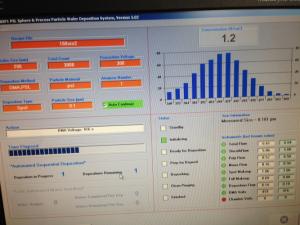
PSL Spheres size standards and silica size standards are scanned by a differential mobility analyzer to determine true size peak. Once the size peak is analyzed, then the wafer standard can be deposited as a full deposition or a spot deposition, or a multiple spot deposition wafer standards. Silica size peak at 100 nano meters (0.1 microns) is scanned above and the DMA detects a true silica size peak at 101nm. Full Deposition or Spot Deposition Wafer Standards – A particle deposition system provides highly accurate, PSL Calibration Wafer Standards and Silica Contamination Wafer Standards. Our 2300 XP1 Particle Deposition System provides automatic particle deposition control to produce your PSL Wafer Standards and Silica Wafer Standards.
Deposit PSL spheres and silica particles on prime silicon wafer standards, or your 150mm photo masks.
Wafer Standards · KLA Surfscan / SSIS Search Path
The inspection-platform name alone does not define the correct reference. Start with the exact tool and recipe, then specify wafer diameter, substrate, particle material and size, and full-wafer or controlled spot deposition.
Inspection-platform context
Current KLA search context: Surfscan SP7XP / SP7, SP5XP / SP5, SP3, SP A3 and SC1. Legacy / mature-tool context: SP2XP, SP2, SP1 variants and earlier Tencor systems.
Compatibility rule: do not infer Applied Physics standard compatibility from platform family alone. Confirm exact tool model, wafer diameter/substrate, particle material, nominal size(s), deposition geometry and recipe objective.
Inspection Tool Intent → Reference Standard
Leading-edge unpatterned-wafer inspection intent. Quote from the exact wafer/substrate, target particle size, deposition geometry and recipe objective; do not reuse an older SP-series configuration by assumption.
High-sensitivity process and tool-monitoring intent. Determine whether the requirement is PSL size-response verification, silica/contamination reference work, or another qualified reference.
Unpatterned-wafer inspection and mature-node support intent. Confirm wafer diameter, substrate, particle material, nominal size and full-versus-spot deposition before quoting.
Installed-base and mature-tool support. Preserve the customer’s known recipe/SOP when available rather than forcing a current-tool configuration onto a legacy system.
Compound-semiconductor inspection intent. Substrate optical response, inspection channel and wafer handling can differ materially from silicon; treat the substrate and recipe as first-class RFQ requirements.
For Hitachi, ADE, Topcon and other inspection systems, identify the exact model and the measurement objective first. AP can then map the request to PSL, silica or another appropriate reference configuration.
Important: these tool families are search and application context, not blanket compatibility claims. The quoted standard must be confirmed against the customer’s actual inspection configuration.
Controlled PSL size-response reference for compatible wafer-inspection workflows.
Use where the process or study calls for silica or another contamination surrogate.
Choose full deposition or controlled spot patterns from the measurement objective and tool recipe.
Reference Selection
| Customer objective | Start with | Critical RFQ variables |
|---|---|---|
| Verify SSIS particle-size response | PSL calibration wafer | Tool/model, wafer, nominal size(s), full vs spot, recipe/SOP |
| Evaluate repeatability / scan response across wafer | Full-deposition calibration wafer | Wafer diameter/substrate, target peak, scan objective |
| Use a non-PSL / silica reference | Silica contamination wafer | Optical method, substrate, size(s), deposition geometry |
| Develop or verify a particle-reference workflow off-wafer | Particle size standard | Material, nominal size, concentration/form, instrument, certificate need |
| Compound semiconductor / SiC / GaN inspection | Configuration review first | Tool/model, substrate, diameter, surface/epi state, channel/recipe objective, reference material |
A model name such as Surfscan SP5, SP7 or SP2 does not uniquely determine the correct standard. Sensitivity mode, substrate, recipe and calibration objective can change the useful reference configuration.
For quoting: include any internal SOP/specification number and whether the standard is for initial calibration, periodic verification, recipe development or troubleshooting.
RFQ Conversion Checklist
Use the product quote control. Your selected product, variation and quantity will remain attached to the request while you add application and technical details.
Technical FAQ
VERIFICATION OBJECTIVE
Challenge detection and sizing response at one or more known particle diameters.
Use controlled deposition across the wafer to evaluate response consistency.
Compare response between scanners, sites or maintenance states using the same reference.
Develop or verify an inspection recipe against a defined particle and substrate condition.
Use silica or another specified material when the study requires a different contamination surrogate.
Particle-size traceability, deposited particle count and deposition geometry are separate attributes. Confirm which values are certified in the quoted documentation.

Enter your details below to save your shopping cart for later. And, who knows, maybe we will even send you a sweet discount code :)
Allow notifications to get real-time updates about your shopping cart and who knows, you may even receive a sweet discount code 😊