
Last Updated: August 10, 2026
Semiconductor manufacturing has reached a critical inflection point. As process nodes shrink below 3 nanometers and high-frequency applications demand unprecedented precision, the margin for error in wafer calibration has effectively disappeared. A single miscalibration can cascade through an entire production run, rendering millions of dollars in silicon unusable.
The semiconductor industry operates on razor-thin tolerances. Feature sizes now measure in single-digit nanometers, while RF and analog circuits push into terahertz frequencies. Applied Physics has spent over three decades helping manufacturers establish and maintain calibration foundations through precision calibration wafer standards and metrology solutions.
What’s changed in 2026 is the regulatory landscape. NIST traceability requirements have tightened, high-frequency characterization standards have evolved, and semiconductor measurement uncertainty specifications have become stricter. Fabs relying on legacy calibration approaches no longer meet current compliance expectations.
Key Takeaway Wafer calibration standards aren’t optional infrastructure. They’re the foundation that makes every downstream measurement trustworthy.
On-wafer calibration embeds the calibration reference directly into the device under test, eliminating systematic errors introduced by probe-to-device transitions. For advanced nodes operating at sub-6 GHz frequencies and beyond, on-wafer calibration is mandatory.

Semiconductor engineer performing on-wafer calibration measurements at a probe station with calibration wafers visible and measurement equipment in a professional cleanroom environment with overhead lighting
The most widely adopted methodology uses 16-term error correction models, which characterize forward and reverse directivity, source and load match, isolation, transmission tracking, and reflection tracking. A proper 16-term calibration eliminates systematic errors down to the noise floor of the vector network analyzer itself.
Setting up on-wafer calibration requires calibration artifacts (typically TRL standards) fabricated on the same wafer as test devices with precisely known electrical characteristics, a probe station capable of making repeatable contact to micrometer-scale features, and measurement firmware that executes the calibration algorithm and stores error terms.
The practical challenge emerges when scaling across production. Each wafer lot introduces subtle variations in metal resistivity, dielectric properties, and substrate characteristics. A calibration valid for one wafer may introduce unacceptable errors on the next. This is where NIST-traceable calibration wafers become essential.
Pro Tip On-wafer calibration artifacts must be measured and characterized before use. Store calibration wafers separately from test wafers to prevent contamination or mechanical damage that would invalidate their reference values.
NIST traceability means your measurements connect to a national standard through an unbroken chain of documented comparisons. A NIST-traceable calibration wafer carries certification that its electrical properties, impedance, thickness, and dielectric constant have been measured against national standards with explicit uncertainty bounds.
Calibration artifacts are only as good as their characterization. A TRL standard claiming 50-ohm impedance but actually measuring 50.3 ohms will systematically bias every measurement made with it. NIST traceability provides documentation proving your standards are what you think they are.
Polystyrene latex (PSL) particles represent one category of NIST-traceable standards used in particle metrology. These monodisperse spheres, available from 20 nanometers to 12 microns, are deposited onto wafers in known quantities. When a scanning surface inspection system measures these particles, the system’s size accuracy and count efficiency can be directly validated against NIST-certified reference values.
For film thickness and optical property measurements, NIST traceability typically involves certification of refractive index, thickness uniformity, and material composition. A certified film thickness standard wafer might specify that a silicon dioxide layer measures 100 nanometers ± 2 nanometers across the entire 300mm surface, with explicit uncertainty analysis.
Applied Physics provides calibration wafer standards in 150mm, 200mm, and 300mm formats, each with NIST-traceable certification. These standards enable fabs to validate their measurement systems against documented national references rather than relying on equipment manufacturer specifications alone. The cost of maintaining NIST-traceable standards is modest compared to the cost of undetected measurement errors.
The 16-term error model has become the industry standard for RF and microwave measurements because it captures the complete systematic error signature of a two-port measurement system. A vector network analyzer doesn’t directly measure S-parameters; it measures incident and reflected voltage waves, then calculates S-parameters mathematically. Systematic errors in that measurement chain, directivity errors, source match errors, load match errors, tracking errors, all distort the calculated S-parameters. The 16-term model quantifies all of these.
The model divides error terms into forward and reverse categories. Forward error terms characterize measurement errors when you excite port 1 and measure port 2. Reverse error terms characterize the opposite direction. Within each direction, the model captures:
Calibrating these 16 terms requires reference standards with known S-parameters. TRL (Thru-Reflect-Line) calibration uses three standards: a Thru standard (direct connection), a Reflect standard (known impedance mismatch), and a Line standard (known length of transmission line). Measuring these three standards and solving the 16-term equations yields the error terms.
The accuracy of S-parameter measurements depends entirely on the accuracy of your calibration standards. A Reflect standard that’s nominally open-circuit but actually has 10 picofarads of stray capacitance will introduce errors into your entire measurement.
Watch Out S-parameter measurements are only valid within the frequency range where your calibration standards have been characterized. Extrapolating beyond that range introduces systematic errors. If you need measurements at terahertz frequencies, your calibration standards must be designed and certified for terahertz operation.
Measurement uncertainty quantifies the doubt inherent in any measurement. It’s not the same as error, an error is a specific, quantifiable deviation, while uncertainty is the range within which the true value probably lies.
Every measurement system has uncertainty sources: instrument noise, calibration standard imperfection, environmental drift, operator technique, and uncorrected systematic errors. Proper uncertainty analysis identifies and quantifies each source, then combines them into a total uncertainty budget.
For semiconductor manufacturing, measurement uncertainty directly impacts yield and process control. If you’re controlling a critical dimension to 10 nanometers and your measurement uncertainty is ±3 nanometers, you’re left with only ±7 nanometers of actual process control margin. Reducing measurement uncertainty from ±3 nanometers to ±1 nanometer effectively triples your process control window.
The semiconductor industry has standardized on Type A uncertainty (from statistical analysis of repeated measurements) and Type B uncertainty (from calibration certificates, equipment specifications, environmental conditions). The combined uncertainty is calculated by combining these sources according to established statistical methods.
NIST-traceable standards contribute to uncertainty control by providing documented uncertainty values. When you use a NIST-traceable calibration wafer, the calibration certificate specifies not just the measured value but also the uncertainty associated with that measurement. Process control requires establishing control limits based on your measurement uncertainty.
Film thickness measurement is foundational to semiconductor manufacturing. Every major process step, oxidation, deposition, etching, depends on controlling film thickness to tight tolerances. Optical metrology dominates film thickness measurement in modern fabs. Spectroscopic ellipsometry measures the polarization change of reflected light to infer film thickness and optical properties. But it requires calibration standards.
A film thickness calibration standard is typically a witness wafer with a deposited film of known thickness, measured using a reference instrument traceable to NIST and documented on a calibration certificate. When you measure this standard with your production measurement tool, you validate that your tool is measuring correctly.
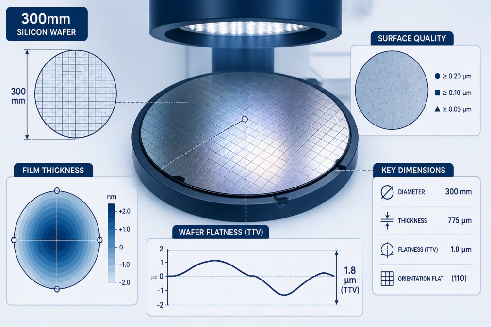
Close-up of a 300mm silicon wafer under inspection lighting showing surface quality and flatness characteristics in a cleanroom environment with soft overhead illumination
Wafer flatness is equally critical. A warped or bowed wafer introduces errors into lithography, deposition, and etching. Flatness is typically specified as Total Thickness Variation (TTV) or Warp, measured in micrometers across the wafer surface.
Interferometry provides the gold standard for flatness measurement. A reference flat, typically an optically polished surface with known flatness, is compared against the wafer surface using interference patterns. Reference flats must themselves be calibrated against NIST-traceable standards.
Modern fabs often use automated optical inspection systems to measure wafer flatness and film thickness simultaneously. These systems require regular calibration against standard wafers to ensure measurement accuracy. Applied Physics provides calibration wafer standards in multiple formats to support both manual and automated measurement systems.
RF calibration wafers are specialized artifacts designed specifically for high-frequency measurements. Unlike general-purpose calibration standards, RF calibration wafers are engineered to deliver accurate S-parameter references across gigahertz to terahertz frequency ranges.
The design of RF calibration structures requires careful attention to parasitic effects. A nominally 50-ohm transmission line might have 0.5 picofarads of fringing capacitance per millimeter. At 100 GHz, that capacitance becomes significant, shifting the effective impedance. RF calibration wafers account for these effects through careful design and characterization.
Probe contact is the most critical source of error in on-wafer RF measurements. A probe touching a calibration structure introduces contact resistance, parasitic inductance, and capacitance. Proper RF calibration wafer design minimizes contact sensitivity through strong contact pad geometry and material selection.
TRL calibration standards for RF work must have precisely known electrical length. A Line standard designed for 40 GHz operation may introduce unacceptable errors at 110 GHz. Best practice dictates fabricating multiple RF calibration wafers with different electrical lengths to cover different frequency ranges. A 500-micrometer line works well for 10-40 GHz. A 250-micrometer line extends the range to 80 GHz. A 100-micrometer line reaches 200 GHz. Each wafer is characterized separately and used only within its intended frequency range.
Environmental stability matters for RF calibration. Temperature changes shift the electrical length of transmission lines through thermal expansion. RF calibration wafers should be stored and used in temperature-controlled environments.
Best For Fabs characterizing advanced RF devices at frequencies above 28 GHz should maintain separate RF calibration wafer sets for each major frequency band (28-40 GHz, 70-90 GHz, 110-150 GHz). This ensures measurement accuracy without relying on extrapolation across wide frequency ranges.
The regulatory environment for semiconductor metrology has shifted significantly in 2026, creating explicit compliance obligations that did not exist in prior years.
FDA Medical Device Guidance (Effective 2026) The FDA’s updated guidance on semiconductor components in Class II and Class III medical devices now requires documented NIST traceability for any measurement supporting a device’s safety or performance claim. Fabs supplying these markets must demonstrate that their measurement systems are calibrated against traceable standards and that calibration records are retained for the device’s entire shelf life plus seven years. Audits by FDA investigators now explicitly request calibration certificates and re-verification records. Non-compliance can result in warning letters, consent decrees, or import alerts.
Automotive ISO 26262 Functional Safety (Phase-In Through 2026) The automotive industry’s adoption of ISO 26262 functional safety standards has created a direct link between measurement system capability and vehicle safety certification. Semiconductor suppliers to Tier 1 automotive suppliers must now provide evidence that their measurement systems meet defined capability indices (typically Cpk ≥ 1.33 for critical parameters). Audits by OEM quality teams now include a specific checklist for calibration standard traceability, verification intervals, and measurement system analysis. Suppliers failing this audit are placed on probation and given 90 days to remediate.
Department of Defense Supply Chain Requirements (Effective January 2026) The DoD’s updated semiconductor supply chain security requirements mandate that all measurement data supporting device acceptance must be traceable to NIST or equivalent national standards. Fabs must maintain a complete audit trail showing: (1) the calibration standard used, (2) the date of calibration, (3) the uncertainty of the standard, (4) the measurement result, and (5) the traceability chain to NIST. Failure to provide complete traceability documentation can result in contract termination and debarment from future DoD contracts.
Calibration Lifecycle Management: Practical Implementation
A calibration standard has a finite useful life, typically 3-5 years depending on usage intensity and storage conditions. Proper lifecycle management includes:
Initial Characterization and Baseline Documentation When a new calibration standard is received, it must be measured and certified by an accredited metrology lab. The certification must include the measured value, measurement uncertainty (typically expressed as an expanded uncertainty with k=2 coverage factor), measurement date, and traceability statement linking the measurement to NIST. This baseline is stored as the reference against which all future measurements are compared.
Drift Detection Through Periodic Re-Verification Re-verification involves measuring the standard again at defined intervals using the same or equivalent measurement method. The new measurement is compared to the baseline. If it falls within the original uncertainty bounds, the standard is deemed stable. If it drifts beyond the uncertainty bounds, the standard shows evidence of degradation. Current best practice recommends:
Documented Storage and Environmental Control Calibration standards must be stored separately from test wafers to prevent contamination or mechanical damage. Storage conditions should include temperature control (20-25°C with ±2°C stability), humidity control (35-65% relative humidity), protection from dust and chemical fumes, and secure storage to prevent unauthorized handling. Each standard should be assigned a unique identification number and tracked in a calibration management database.
Drift Threshold and Retirement Criteria A standard is retired when re-verification shows drift exceeding a defined threshold, typically set at 50% of the original measurement uncertainty. Retiring a standard before it fails prevents the risk of undetected degradation affecting production. Retired standards should be archived for a minimum of seven years before disposal.
Complete Traceability Documentation and Audit Trail Every measurement made with a calibration standard must be documented with the standard’s identification number and certification date, measurement date and time, measurement result, measurement system used, operator identification, and any environmental conditions that might affect the measurement. This documentation creates a complete audit trail demonstrating traceability from the production measurement back through the calibration standard to NIST.
2026 Compliance Checklist for Fabs To ensure compliance with 2026 regulatory requirements, fabs should:
Applied Physics supports this lifecycle through calibration wafer standards with comprehensive documentation packages. Each standard comes with initial NIST-traceable certification, and customers can arrange periodic re-verification through qualified metrology labs.
Selecting calibration standards requires balancing precision against cost and maintenance burden. The right choice depends on your specific manufacturing requirements, production volume, and regulatory obligations.
Step 1: Define Your Measurement Uncertainty Target Start by working backward from your device specifications and process control requirements. A common allocation rule is to assign 30% of the total uncertainty budget to the calibration standard. If your total budget is ±0.3 dB, the calibration standard should contribute no more than ±0.09 dB of uncertainty.
Step 2: Map Uncertainty Requirements to Standard Grade Calibration standards are available in several grades:
Grade 1 (Precision Reference Standards): Uncertainty ±0.5% or better. Used for critical measurements where tight process control directly impacts yield. Verification interval: quarterly.
Grade 2 (Working Standards): Uncertainty ±1-2%. Used for routine measurements where moderate process control is sufficient. Verification interval: semi-annual.
Grade 3 (Check Standards): Uncertainty ±3-5%. Used for periodic system verification and trending. Verification interval: annual.
Step 3: Calculate the Cost of Measurement Error The financial justification for a calibration standard depends on the cost of measurement error. Without proper calibration, undetected measurement errors manifest as customer returns or yield loss. A Grade 1 RF calibration standard costing $12,000 that prevents $25,000 in monthly customer returns pays for itself in less than one month.
Step 4: Account for Lifecycle and Maintenance Costs The total cost of a calibration standard includes purchase price, re-verification, storage, and eventual retirement. A Grade 1 standard with a $12,000 purchase price has a 5-year total cost of ownership of approximately $25,000-$35,000 when including re-verification and maintenance.
Step 5: Implement a Tiered Calibration Strategy Most semiconductor fabs optimize cost by using a tiered approach:
Tier 1 (Precision Standards): Used for critical measurements that directly impact yield or device performance. Maintained with rigorous lifecycle management (quarterly re-verification).
Tier 2 (Working Standards): Used for routine measurements where moderate process control is sufficient. Maintained with standard lifecycle management (semi-annual re-verification).
Tier 3 (Check Standards): Used for periodic system verification and trending. Maintained with minimal lifecycle management (annual re-verification).
This tiered approach typically reduces overall calibration costs by 40-50% compared to maintaining all standards at Grade 1 precision, while still protecting against measurement errors that would impact production.
Step 6: Justify the Investment to Finance and Operations When presenting a calibration standard investment, frame it in terms of risk and return. Quantify the cost of undetected measurement error in terms of yield loss, rework, customer returns, or regulatory penalties. Quantify how much the calibration standard reduces that risk. Most Grade 1 standards pay for themselves within 3-6 months in high-volume production.
Common Pitfalls to Avoid
Underestimating the Cost of Measurement Error: Many fabs focus on the visible cost of calibration standards while ignoring the hidden cost of poor measurement. Conduct a root cause analysis on recent quality issues to quantify the true cost.
Overspecifying Precision: Purchasing Grade 1 standards for all measurements is wasteful. A Grade 2 standard is sufficient for most routine measurements. Reserve Grade 1 for critical measurements where the cost of error is highest.
Neglecting Lifecycle Management: Without proper re-verification and retirement procedures, the standard will degrade over time and introduce errors into your measurements. Budget for lifecycle management as part of the total cost of ownership.
Ignoring Environmental Factors: A calibration standard stored in an uncontrolled environment will degrade faster and require more frequent re-verification. Proper storage infrastructure is part of the investment.
Applied Physics provides calibration wafer standards in 150mm, 200mm, and 300mm formats, enabling fabs to scale their calibration infrastructure from R&D through high-volume production. Our tiered product line allows you to match your calibration investment to your production scale and measurement criticality. Contact our metrology specialists to conduct a cost-benefit analysis for your specific manufacturing environment.
NIST provides traceability frameworks for calibration standards rather than a single ‘NIST standard’ for wafers. NIST-traceable calibration wafers are certified artifacts with documented particle sizes, film thicknesses, or electrical properties linked to national measurement standards. For semiconductor applications, NIST traceability ensures that your metrology instruments measure accurately against recognized benchmarks. This traceability is critical for 2026 compliance, as manufacturers must demonstrate measurement uncertainty within defined limits for advanced node production at 5nm and below.
NIST traceability establishes a chain of custody for measurement accuracy that regulators and customers require. As semiconductor nodes shrink, measurement uncertainty becomes a larger percentage of the feature size, at 3nm, a 0.5nm uncertainty is significant. NIST-traceable standards allow you to prove that your metrology is accurate within defined limits, which is essential for process control, yield optimization, and regulatory audits. Without traceability, you cannot confidently claim that your measurements are valid for advanced manufacturing or pass third-party qualification audits.
RF calibration wafers are designed for high-frequency characterization and include S-parameter artifacts, transmission line structures, and impedance standards that operate at gigahertz frequencies. DC calibration wafers focus on electrical properties at direct current, such as resistivity, doping profiles, and contact resistance. RF calibration wafers are essential for mm-wave and terahertz device development, while DC standards support traditional transistor modeling and process monitoring. The choice depends on your device type: RF wafers for communication and sensing devices, DC wafers for logic and memory.
Recertification intervals depend on the standard type and your process requirements. Most NIST-traceable particle standards (PSL wafers) should be recertified annually or after significant process changes. Film thickness and flatness standards typically require recertification every 12-24 months, depending on usage intensity and storage conditions. For 2026 compliance, document your recertification schedule and maintain certificates on file. More frequent recertification may be justified if your process is near specification limits or if you operate in high-volume manufacturing where measurement drift directly impacts yield.
APPLIED PHYSICS TECHNICAL RESOURCE
Wafer inspection, SSIS calibration, particle deposition references, process control and semiconductor measurement workflows. Product and standards references should be interpreted for the actual instrument, facility, protocol and configuration.

Enter your details below to save your shopping cart for later. And, who knows, maybe we will even send you a sweet discount code :)
Allow notifications to get real-time updates about your shopping cart and who knows, you may even receive a sweet discount code 😊