
Last Updated: August 5, 2026
Semiconductor yield improvement metrology has become the defining challenge for modern fabs. At Applied Physics, we’ve analyzed thousands of production runs across multiple nodes, and the pattern is unmistakable: facilities that treat metrology as a strategic function, not an afterthought, consistently outperform competitors on both yield and cycle time.
The economics are brutal. A single percentage point of yield loss on a 300mm wafer fab can cost millions annually. Yet most facilities operate with metrology systems that were adequate five years ago but are fundamentally misaligned with today’s manufacturing realities. Sub-10nm process nodes demand measurement uncertainty below 2nm. Older systems simply cannot deliver that precision.
Yield improvement metrology isn’t just about catching defects. It’s about understanding process variation at the wafer-level, identifying root cause patterns before they propagate through your fab, and accelerating your yield ramp when you transition to new nodes. The difference between a facility that ramps to target yield in six months versus twelve months often comes down to metrology infrastructure.
Pro Tip The real competitive advantage isn’t in the inspection tool itself, it’s in how you interpret the data it generates. Facilities that combine in-line metrology with advanced statistical process control see yield improvements 30-40% faster than those relying on traditional off-line sampling.
When you’re evaluating a metrology upgrade, the conversation with finance usually stalls at capital cost. That’s the wrong lens entirely. The real ROI calculation involves three components: yield acceleration, defect density reduction, and cycle time compression.
A typical metrology system upgrade costs between $500,000 and $2 million depending on your node and wafer size. That sounds large until you model the impact. If an upgrade accelerates your yield ramp by six weeks, you’re looking at 30,000-50,000 additional wafers reaching target yield per year. At $5,000-$15,000 net margin per wafer, that’s $150-750 million in incremental revenue. The payback period is typically 2-4 weeks.
The harder metric to quantify is defect density reduction. When you transition from monthly off-line sampling to real-time in-line metrology, you catch systematic defects within hours instead of weeks. This prevents scrap of thousands of wafers. Most facilities underestimate this component by 40-60% because they don’t track the wafers that would have failed inspection downstream.
Cycle time compression is the third lever. Advanced metrology systems provide feedback fast enough to enable same-day process adjustments. Facilities that implement this see fab throughput improvements of 8-12% without adding equipment. That’s pure margin expansion.
Watch Out The biggest mistake in ROI analysis is treating metrology as a cost center rather than a revenue driver. If your finance team is asking “what’s the minimum we can spend on metrology,” you’re already losing money compared to competitors who view it as yield infrastructure.
Yield ramp is the period between process qualification and reaching target yield. For advanced nodes, this window has compressed from 12 months to 6-8 months, but only for facilities with precision metrology infrastructure.
The mechanism is straightforward: yield improvement metrology provides the data density you need to identify which process parameters actually drive yield. Without this data, ramp acceleration is guesswork. You adjust temperature, pressure, or chemistry based on intuition. With high-resolution metrology, you see the statistical relationship between each parameter and defect formation.
Applied Physics calibration wafer standards are designed specifically for this purpose. They provide traceable reference points across multiple wafer sizes (100mm through 300mm) so your metrology tools maintain accuracy throughout the learning phase. This prevents the common scenario where your yield data becomes increasingly unreliable as your tools drift over weeks of intensive characterization.
The yield learning process typically follows this sequence: First, establish baseline defect signatures using in-line inspection. Second, correlate defect locations to specific process steps using root cause analysis. Third, adjust process parameters and measure the impact within 24 hours. Fourth, validate improvements across multiple lots before scaling. Facilities that compress this cycle to 48-hour iterations reach target yield 8-10 weeks faster than those using weekly sampling.
Statistical process control is essential here. You’re not just collecting data, you’re identifying which variations are noise and which signal actual process drift. The difference between a facility that controls critical dimension to ±2nm and one that controls to ±5nm is often just discipline in interpreting metrology output.
Defect detection and characterization sits at the intersection of hardware capability and analytical rigor. The inspection tool generates images. The data science determines whether those images represent real defects or false positives.
Modern semiconductor defect inspection systems use multiple detection modalities. Bright field imaging catches metal and dielectric defects. Dark field catches particle contamination and subtle surface anomalies. Laser scanning finds micro-cracks and delamination. No single modality catches everything. Facilities that layer multiple inspection techniques across different process steps achieve defect capture rates above 95%. Those relying on single-modality tools typically miss 20-30% of defects that emerge as yield loss downstream.
The characterization step is where most facilities struggle. You’ve detected a defect, now what? Is it a killer defect that guarantees circuit failure, or a benign artifact? Does it originate from wafer environment contamination, or from tool drift? Answering these questions requires correlating defect location with electrical test data, process parameters, and equipment logs.
Automated defect classification (ADC) has improved dramatically in the last three years. Machine learning models trained on thousands of labeled defects can now predict electrical impact with 85-90% accuracy. But the models are only as good as the training data. Facilities that invest in rigorous defect labeling, correlating inspection images to actual yield loss, build classification systems that drive real process decisions.
Root cause analysis is the final step. You’ve identified a defect population. Now trace it back: which tool, which shift, which material lot, which process recipe? Wafer map analysis combined with equipment sensor data usually points to the culprit within 2-3 iterations.
Key Takeaway The facilities winning on yield ramp are those treating defect characterization as a continuous learning process, not a one-time qualification activity. Each defect teaches you something about your process, but only if you’re structured to capture that learning.
Contamination is the silent yield killer. A single particle of 0.5 micrometers can bridge a critical dimension gap and cause circuit failure. Yet most fabs have only monthly visibility into particle levels in their cleanrooms.
Particle metrology has evolved from periodic sampling to real-time monitoring. Advanced particle counters can detect particles down to 0.1 micrometers and provide location-specific data. This transforms contamination control from reactive (“we had a problem, now we’re fixing it”) to predictive (“we’re seeing early signs of a contamination event, let’s prevent it”).
The challenge is that particle metrology data is often disconnected from wafer yield data. You know your cleanroom has elevated particles, but you don’t know which wafers were exposed or which process steps are most vulnerable. Facilities that integrate particle monitoring with wafer movement tracking can identify exactly which lots were at risk and adjust their yield models accordingly.
Wafer environment contamination control requires understanding your specific vulnerability. For some fabs, the primary risk is airborne particles. For others, it’s mobile ionic contamination from process chemistry. For advanced packaging, it’s solder flux residue. The metrology approach differs for each. Applied Physics helps fabs establish particle metrology baselines and track trends over time using calibrated standards.
One often-overlooked aspect: contamination events often appear as yield loss 2-4 weeks after exposure. By the time you see the yield impact, the contamination source is gone and root cause analysis becomes guesswork. Real-time particle metrology lets you correlate the event to actual wafer exposure, compressing your investigation timeline from weeks to hours.
The shift from off-line to in-line metrology is perhaps the most significant change in fab operations over the last decade. Yet many facilities still treat them as competing approaches rather than complementary ones. The real decision isn’t binary, it’s about understanding the economic and operational trade-offs for each critical process step.
In-Line Metrology: Real-Time Feedback at a Cost
In-line metrology measures wafers immediately after a process step while they remain in the tool queue. This enables same-day process adjustments and prevents systematic defects from propagating through your fab. The measurement happens in seconds to minutes, and results feed directly into advanced process control (APC) systems that can adjust tool parameters before the next wafer enters.
The throughput cost is substantial. A typical in-line critical dimension (CD) measurement adds 8-15 minutes of fab time per wafer. For a 300mm fab running 200 wafers per day, that’s 27-50 hours of additional tool time daily. At $500-$1,000 per hour of fab throughput cost, that’s $13,500-$50,000 in daily opportunity cost. This is why in-line metrology is deployed selectively, not universally.
The yield benefit justifies this cost only when the process step is critical and prone to drift. Lithography overlay, etch CD, and deposition thickness are typical candidates. A 0.5% yield loss prevented by catching overlay drift within hours instead of days easily justifies the throughput cost. A 0.05% yield loss does not.
Defect escape rate is the key metric. In-line metrology typically reduces defect escape (defects that pass in-line inspection but fail downstream electrical test) by 40-60% compared to off-line sampling. This is because you’re measuring 100% of wafers in real time, not sampling 5-10% weekly. The statistical power to detect systematic defects is orders of magnitude higher.
Off-Line Metrology: Comprehensive Characterization Without Throughput Impact
Off-line metrology removes wafers from production flow and measures them in a dedicated metrology lab. This eliminates throughput impact and allows comprehensive characterization: cross-sectional scanning electron microscopy (SEM), atomic force microscopy (AFM), transmission electron microscopy (TEM), and spectroscopic analysis. These techniques provide defect root cause information that in-line tools cannot deliver.
The latency cost is severe. A typical off-line measurement cycle is 24-72 hours from wafer removal to results. By the time you receive data, you’ve already processed 500-2,000 wafers with potentially drifted parameters. This makes off-line metrology unsuitable for real-time process control. Instead, it serves periodic validation and root cause investigation.
Off-line metrology is essential for yield learning during ramp. When you’re trying to understand which process parameters drive defect formation, you need the detailed characterization that SEM and AFM provide. You cannot correlate a defect to a root cause with optical CD measurements alone. The investment in off-line infrastructure during ramp (typically 6-12 months) pays dividends in accelerated learning.
Off-line measurement uncertainty is typically lower than in-line (±0.5nm vs ±1-2nm for CD) because you have time for multiple measurements, environmental control, and advanced analysis techniques. This makes off-line data the gold standard for validating in-line tool calibration.
The Hybrid Deployment Strategy: Where to Use Each
Best-in-class fabs use a structured decision matrix:
Deploy in-line metrology when:
Typical in-line candidates: post-lithography CD, post-etch CD, post-deposition thickness, overlay after alignment steps.
Deploy off-line metrology when:
Typical off-line candidates: defect characterization, cross-sectional analysis, periodic validation of in-line tools, root cause investigation of yield loss events.
Quantifying the Economic Trade-Off
The decision framework requires three calculations:
Throughput cost of in-line measurement: (Measurement time in hours) × (Wafers per day) × (Fab throughput cost per hour). For a 300mm fab with 200 wafers/day and $750/hour throughput cost, a 12-minute measurement costs $30,000 daily or $10.95 million annually.
Yield benefit from real-time feedback: (Defect escape rate reduction) × (Wafers per year) × (Cost per defective wafer). If in-line metrology reduces escape rate from 5% to 2%, and each defective wafer costs $8,000 in scrap and rework, the annual benefit is (3% × 73,000 wafers × $8,000) = $17.52 million.
Payback period: Yield benefit minus throughput cost. In this example, $17.52M – $10.95M = $6.57M annual net benefit, or a payback period of 6-8 weeks.
This calculation is process-specific. A process step with low yield impact (0.5% defect escape reduction) will not justify in-line metrology. A process step with high yield impact (3-5% defect escape reduction) almost always will.
Implementation Sequencing
Most advanced fabs implement a phased approach:
The facilities seeing the fastest yield ramp are those that use off-line data to guide in-line tool placement. If off-line SEM analysis shows that 80% of defects originate from a specific process step, that’s where you deploy in-line metrology first. Let the data guide your investment.
Pro Tip The biggest mistake in metrology deployment is treating in-line and off-line as competing choices. They are complementary. In-line catches systematic defects in real time. Off-line provides the root cause understanding that prevents those defects from occurring in the first place. Deploy both, but sequence them based on your yield data, not on budget availability.
Advanced semiconductor defect inspection systems have become so sophisticated that the limiting factor is usually interpretation, not detection. Modern tools can identify defects at the nanometer scale, but determining which defects matter requires data science discipline.
The current generation of inspection systems uses multiple detection modalities simultaneously. Bright field and dark field imaging capture different defect signatures. Laser scanning adds another dimension. Some systems now incorporate spectroscopy to identify material composition. The result is a rich dataset, but only if you know how to use it.
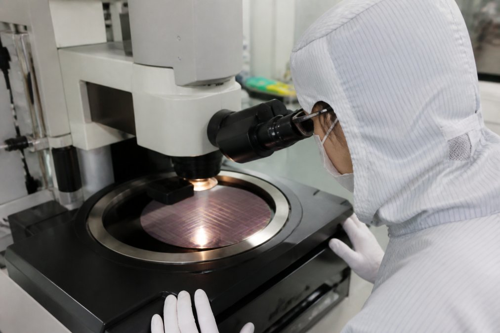
Process engineer examining semiconductor wafer under advanced inspection equipment in cleanroom, with illuminated defect markers visible on wafer surface under precise lighting
Automated defect classification (ADC) has reached a maturity where it’s now a standard tool in most advanced fabs. The models are trained on thousands of labeled defects from your specific process. They learn which defect signatures correlate with yield loss and which are benign. When a new defect appears, the model predicts its electrical impact with reasonable confidence.
The key to effective ADC is continuous model refinement. As you gather more yield data, you update your training sets. Defects you thought were benign might show up as failure modes in electrical test. Conversely, some defects you were worried about never cause problems. The model learns from this feedback.
One critical limitation: ADC models trained on 7nm data don’t transfer well to 5nm processes. The defect signatures change. The criticality changes. You need to retrain your models for each new node. Facilities that understand this invest in strong defect labeling infrastructure, they know the model is only as good as the training data.
Process optimization at advanced nodes lives or dies on metrology precision. Critical dimension control is the foundation. Overlay accuracy is the differentiator.
Critical dimension metrology measures the width of features on your wafer. For 5nm nodes, you’re controlling features to 5nm ±2nm. That’s a tolerance of 40%. Any measurement uncertainty above 0.5nm becomes a significant source of yield loss. This is why sub-10nm calibration wafer standards are non-negotiable for advanced fabs.
Overlay metrology measures how precisely each layer aligns to the previous layer. Misalignment of just 5nm can cause shorts or opens. Modern overlay metrology uses target-based or image-based techniques. Target-based is faster but less precise. Image-based provides better accuracy but requires more processing time. Most advanced fabs use both, target-based for real-time feedback, image-based for periodic validation.
The correlation between metrology precision and yield is direct and quantifiable. Improving critical dimension control from ±3nm to ±2nm typically reduces yield loss by 2-4 percentage points. Improving overlay control from ±4nm to ±3nm prevents 1-2% of defects. These improvements compound across all layers of your process.
Process optimization using metrology follows this pattern: Establish baseline critical dimension and overlay distributions. Identify which process parameters drive variation in each. Run designed experiments varying those parameters while measuring the impact on critical dimension and overlay. Identify the sweet spot that minimizes variation while maintaining target values. Lock those parameters and monitor for drift.
Applied Physics calibration wafer standards provide the reference points you need for this optimization. They’re available in multiple sizes (100mm through 300mm) and can be customized for your specific measurement targets.
Wafer map analysis is where yield improvement metrology transitions from data collection to decision-making. A wafer map shows you where defects are located on a wafer. Patterns in those locations tell you what’s actually happening in your process.

Technician reviewing wafer mapping data on high-resolution monitor in semiconductor fab control room, with multiple data screens displaying process parameters and color-coded defect distributions
Random defect distributions suggest process noise, inherent variation you need to control statistically. Clustered defects at specific locations suggest systematic issues. Edge defects often indicate edge exclusion problems or edge bead removal issues. Ring patterns suggest tool-specific problems that rotate with wafer position. Each pattern tells a story about what’s failing in your fab.
Statistical process control (SPC) is the framework that turns wafer maps into action. You establish control limits based on historical data. When defect density exceeds those limits, you investigate. When defect locations shift, you investigate. When the distribution changes from random to clustered, you investigate. The discipline is in making these investigations systematic rather than reactive.
Advanced fabs implement multi-level SPC. Lot-level SPC tracks defect density across lots. Wafer-level SPC identifies which wafers within a lot are outliers. Intra-wafer SPC identifies which regions of the wafer are problematic. This layered approach helps you isolate problems quickly, is it a tool issue (affects all lots), a material lot issue (affects specific lots), or a processing issue (affects specific wafers or regions)?
Machine learning is now enhancing traditional SPC. Instead of simple control limits, you can build predictive models that identify which combinations of process parameters predict yield loss. These models adapt as your process evolves, unlike fixed control limits that become stale.
Pro Tip The facilities seeing the fastest yield ramp are those using wafer map analysis not just to identify problems, but to guide the design of experiments. If your maps show edge defects, your next DOE should focus on edge exclusion parameters. If your maps show random defects, focus on process noise sources. Let the data guide your investigation.
Measurement uncertainty is the fundamental limit on how well you can control your process. If your metrology tool has 1nm uncertainty, you cannot reliably control critical dimension to better than ±1nm. This is the hard physics of measurement. Understanding where uncertainty becomes a yield killer, and how to reduce it, is the difference between fabs that ramp to target yield in 6 months and those that take 12.
The Uncertainty-Yield Relationship: When Does It Matter?
The relationship between measurement uncertainty and yield loss is quantifiable. For a process with a target critical dimension of 20nm and a process window of ±2nm (10% tolerance), measurement uncertainty of 0.5nm translates to a 25% reduction in your effective process window. You think you’re controlling to ±2nm, but your actual control window is ±1.5nm because you cannot distinguish true process variation from measurement noise.
For sub-7nm nodes, this becomes acute. A 5nm target with ±0.5nm tolerance (10% window) and 0.3nm measurement uncertainty leaves you with an effective window of ±0.2nm. You’re operating at the edge of your process capability, and measurement uncertainty is consuming 60% of your available margin. This is why sub-10nm fabs spend millions on uncertainty reduction, it directly translates to yield.
The yield impact follows a predictable pattern:
For a 5nm node with a 1nm process window, 0.3nm measurement uncertainty is acceptable (30% of window). 0.5nm uncertainty is problematic (50% of window). This is why advanced fabs invest in calibration standards and measurement validation, the ROI is direct and substantial.
Sources of Measurement Uncertainty and Reduction Strategies
Measurement uncertainty comes from multiple sources, each requiring different mitigation:
Instrument calibration drift: Your metrology tool’s accuracy degrades over time due to thermal drift, optical aberration, and mechanical wear. Mitigation: Daily calibration using traceable standards (NIST-traceable calibration wafers), environmental control (±0.5°C temperature stability), and periodic instrument maintenance. Cost: $50,000-$150,000 annually per tool. Uncertainty reduction: 30-50%.
Environmental variation: Temperature, humidity, and vibration affect measurement accuracy. A 1°C temperature change can shift optical measurements by 0.2-0.5nm. Mitigation: Dedicated metrology labs with environmental control (±0.5°C, ±5% RH), vibration isolation tables, and thermal stabilization of samples before measurement. Cost: $200,000-$500,000 for lab infrastructure. Uncertainty reduction: 40-60%.
Sample preparation artifacts: How you prepare the wafer for measurement affects results. Cross-sectional SEM requires cutting the wafer, which can introduce damage. Optical measurements are sensitive to surface cleanliness. Mitigation: Standardized sample preparation protocols, automated cleaning systems, and trained technicians. Cost: $100,000-$300,000 for equipment and training. Uncertainty reduction: 20-40%.
Measurement technique limitations: Different techniques have inherent uncertainty. Optical CD measurements have ±0.5-1nm uncertainty. SEM-based CD has ±0.3-0.5nm. AFM has ±0.1-0.2nm but is slow (30+ minutes per sample). Mitigation: Use the right technique for the application. For real-time control, accept optical uncertainty. For validation, use SEM or AFM. Cost: Varies by technique. Uncertainty reduction: Technique-dependent.
Sampling variation: If you measure only 5 wafers per lot, your sample mean has high uncertainty. Measuring 20 wafers reduces uncertainty by √4 = 2×. Mitigation: Increase sampling rate, but this increases cost. For in-line metrology, measure 100% of wafers. For off-line validation, measure at least 10-15 wafers per lot. Cost: Proportional to sampling rate. Uncertainty reduction: √(n) where n is sample size.
Sensor Fusion: Combining Multiple Measurements to Reduce Uncertainty
Sensor fusion combines data from multiple measurement modalities to reduce overall uncertainty below what any single technique can achieve. Instead of trusting a single optical CD measurement, you combine data from bright field imaging, dark field imaging, and spectroscopy. The ensemble measurement has lower uncertainty than any single modality.
A practical example: Measuring the CD of a 20nm metal line.
If you treat these as independent measurements and average them, your ensemble measurement is 20.33nm with uncertainty of √((0.8² + 0.7² + 0.4²)/9) = 0.35nm. This is better than any single measurement.
But sensor fusion goes deeper. You can weight each measurement by its confidence (inverse of uncertainty). You can identify and reject outliers. You can use machine learning to predict which measurement modality is most reliable for each specific sample based on signal quality and environmental conditions.
Advanced fabs implement sensor fusion at two levels:
Real-time fusion in-line: Combine bright field and dark field measurements from the same optical tool. Reduce uncertainty from ±1nm to ±0.7nm. Cost: Software integration, minimal hardware cost. Payback: 2-4 weeks from improved yield.
Cross-tool validation fusion: Combine in-line optical measurements with periodic off-line SEM measurements. Use the SEM data to identify systematic biases in the optical tool and correct them. Reduce optical uncertainty from ±1nm to ±0.6nm. Cost: Periodic SEM measurements ($500-$1,000 per sample). Payback: 4-8 weeks from improved process control.
Machine Learning for Adaptive Uncertainty Estimation
Traditional metrology assumes measurement uncertainty is constant. In reality, it varies based on signal quality, environmental conditions, and sample characteristics. A measurement taken at 9 AM after the lab has stabilized has lower uncertainty than one taken at 8 AM when the lab is still warming up.
Machine learning models can predict uncertainty for each specific measurement. You train a model on historical data that includes measurement value, signal quality metrics, environmental conditions, and actual defect outcomes. The model learns which conditions produce reliable measurements and which produce noisy ones.
The practical benefit: You can weight high-confidence measurements more heavily in your process control decisions. If a measurement has predicted uncertainty of ±0.3nm, you trust it more than one with ±0.8nm. This allows you to tighten your process control window without increasing false alarm rates.
Implementation cost: $200,000-$500,000 for model development and integration. Payback: 8-12 weeks from improved process stability and reduced false adjustments.
Calibration Standards and Traceability: The Foundation
All uncertainty reduction ultimately depends on calibration. Your metrology tools must be traceable to NIST standards. This isn’t bureaucracy, it ensures that your measurements are meaningful and reproducible across tools, shifts, and years.
Calibration wafer standards provide reference measurements across multiple techniques. A single standard can be measured by optical CD tools, SEM, AFM, and spectroscopy. If all tools agree on the standard, you have confidence in their relative accuracy. If they disagree, you’ve identified a systematic bias that needs correction.
For advanced nodes, calibration standards must be available in multiple sizes (100mm through 300mm) and must cover the specific measurement targets relevant to your process (CD, overlay, thickness, etc.). The cost of a comprehensive calibration standard set is $50,000-$200,000, but the ROI is substantial, it prevents millions in yield loss from undetected tool drift.
Practical Uncertainty Reduction Roadmap
Most fabs follow this sequence:
The cumulative effect: Measurement uncertainty reduction from ±1.2nm to ±0.5nm, a 60% improvement. For a 5nm process, this translates to 2-4% yield improvement and 4-6 week faster ramp.
Watch Out The biggest mistake in uncertainty reduction is treating it as a one-time project. Measurement uncertainty degrades over time as tools drift and standards age. Establish a continuous calibration and validation program. Budget 5-10% of your metrology capital for ongoing uncertainty management. The alternative is slow, undetected tool drift that silently erodes yield over months.
Implementing a world-class metrology system is a multi-year journey, not a one-time project. The best-performing fabs treat metrology as continuous improvement, not a fixed state.
Start with a metrology audit. Map your current measurement capabilities against your process requirements. Identify gaps, where are you measuring with inadequate precision? Where are you not measuring at all? Quantify the yield impact of each gap.
Second, establish measurement traceability. Every metrology system must trace back to NIST standards. This isn’t bureaucracy, it ensures that your measurements are meaningful and reproducible. Applied Physics calibration wafer standards provide this traceability across multiple wafer sizes and measurement targets.
Third, implement real-time feedback loops. Your metrology data should flow directly into process control systems. When a measurement indicates drift, your tools should adjust automatically. This requires integration between your metrology infrastructure and your fab automation systems.
Fourth, establish defect learning protocols. When you see a defect, you should systematically investigate: What is it? Where did it come from? How did it slip through your process controls? What’s the fix? Document these investigations and use them to improve your process understanding.
Fifth, validate your metrology regularly. Use round-robin measurements where multiple tools measure the same wafer. Use cross-correlation between in-line and off-line measurements. Use statistical analysis to identify tool drift before it impacts yield.
The implementation timeline is typically 12-24 months for a major upgrade. Start with critical process steps. Expand to secondary steps as you build confidence. The payback usually begins within 3-6 months as yield improvements compound.
Advanced packaging (2.5D and 3D integration) introduces measurement challenges that traditional wafer metrology doesn’t address. You’re no longer measuring flat wafers, you’re measuring stacked dies, through-silicon vias (TSVs), and micro-bumps.
TSV metrology is particularly challenging. You need to measure via depth, sidewall roughness, and fill quality. Traditional optical metrology struggles because the via is a narrow hole. Acoustic metrology works better but requires different calibration approaches. X-ray metrology provides the best accuracy but is slow and expensive.
Micro-bump metrology requires measuring bump height, diameter, and composition. These are critical for chiplet-to-chiplet connectivity. Variation of just 2-3 micrometers can cause electrical failures. Optical metrology combined with acoustic measurement provides reasonable accuracy, but throughput is a challenge.
Die-to-die alignment in 3D stacks is another critical measurement. You need sub-micrometer accuracy across the entire stack. This typically requires X-ray metrology or advanced optical techniques. The measurement time is significant, sometimes 30-60 seconds per unit, which limits throughput.
Yield improvement metrology in advanced packaging is still evolving. Most fabs are still learning which measurements matter most. This is an opportunity for facilities that invest in comprehensive metrology infrastructure now, they’ll have the data and experience to optimize their processes faster than competitors.
Semiconductor metrology systems consume significant energy. A large fab might have 100+ metrology tools running continuously, each consuming 5-15 kilowatts. That’s 500+ kilowatts just for metrology, equivalent to the power consumption of 400 homes.
Energy-efficient metrology design is becoming a competitive factor. Newer tools use LED illumination instead of xenon lamps, reducing power consumption by 60-70%. Solid-state detectors are more efficient than traditional photomultiplier tubes. Optimized optical designs reduce light loss.
Beyond hardware efficiency, software optimization matters. Smarter algorithms can reduce measurement time per wafer, which reduces tool use and energy consumption. Machine learning models that predict which wafers need detailed measurement versus quick screening can reduce overall metrology throughput by 20-30%.
The sustainability angle extends to calibration standards. Applied Physics calibration wafer standards are designed for durability and long-term use. A single standard can be used for thousands of calibration cycles without degradation. This reduces waste and energy consumption compared to consumable standards that require frequent replacement.
Some fabs are exploring renewable energy to power their metrology infrastructure. Solar panels, wind power, or grid-connected renewable energy can offset the substantial electricity consumption. For a large fab, this can reduce energy costs by 10-15% while improving sustainability metrics.
The business case for energy-efficient metrology is straightforward: lower operating costs and reduced carbon footprint. For fabs with sustainability commitments, this is increasingly important for customer relationships and regulatory compliance.
Semiconductor yield improvement metrology is no longer a supporting function, it’s the core of competitive advantage in advanced manufacturing. Facilities that treat metrology as strategic infrastructure, not as a cost center, consistently outperform on both yield and cycle time.
The path forward requires commitment across three dimensions: capital investment in modern metrology tools, organizational discipline in data interpretation and process control, and continuous learning as your process evolves. Applied Physics supports this journey with calibration wafer standards across all major wafer sizes (100mm, 125mm, 150mm, 200mm, and 300mm) and precision contamination control solutions designed specifically for semiconductor environments. Our 34 years of experience serving the semiconductor industry means we understand the measurement precision and traceability your fab requires. Get started with Applied Physics and transform your metrology from a bottleneck into a competitive advantage.
Metrology enables yield improvement by detecting defects early, characterizing process variations, and providing data-driven insights into root causes of yield loss. In-line metrology systems capture real-time measurements of critical dimensions, overlay accuracy, and contamination levels, allowing engineers to adjust process parameters before defects propagate. This precision measurement capability reduces wafer-to-wafer variability and accelerates yield ramp during new node transitions, directly impacting fab throughput and profitability.
Yield is calculated as (number of functional dies per wafer / total dies per wafer) × 100%. Fab-level yield accounts for all defects, from process-induced critical dimension errors to contamination-related faults. Metrology data feeds this calculation by identifying which defects are systematic (repeatable across multiple wafers) versus random. Tracking yield by defect type and location on the wafer map reveals which process parameters need adjustment, enabling targeted improvements that increase overall fab yield.
Common techniques include optical critical dimension (CD) metrology for feature sizing, overlay metrology for layer alignment, thin film measurement for deposition thickness, and automated defect classification (ADC) for pattern-based inspection. Advanced fabs also deploy machine learning-enhanced systems for signal-to-noise ratio optimization and sensor fusion to combine multiple measurement types. In-line metrology captures data during production, while off-line metrology (including calibration wafer standards) validates process stability and supports root cause analysis without interrupting fab throughput.
Effective wafer metrology reduces cycle time by catching yield loss mechanisms early, preventing scrap of partially processed wafers. In-line systems provide immediate feedback, enabling real-time process adjustments that minimize defect density before downstream steps. Off-line metrology using calibration wafer standards validates process control without consuming production capacity. When implemented correctly, metrology investments reduce rework, lower fab downtime, and accelerate yield ramp, ultimately increasing throughput per unit of cleanroom space and equipment.
Inspection detects the presence of defects and classifies them by type (e.g., bridging, missing features, contamination). Metrology measures specific parameters, critical dimension, overlay, thickness, or particle count, to quantify process performance. Inspection answers ‘Is there a defect?’ while metrology answers ‘What is the exact measurement, and does it meet specification?’ Together, they enable root cause analysis: inspection identifies where yield loss occurs, and metrology reveals why, allowing engineers to optimize process parameters and reduce yield loss mechanisms.
Smaller fabs benefit most from calibration wafer standards and targeted in-line metrology that focus on the highest-risk process steps. Calculate ROI by quantifying yield loss in dollars, a 2-3% yield improvement on a 300mm wafer fab with 10,000 wafers per month translates to significant revenue recovery. Start with off-line metrology to validate process control without capital-intensive equipment, then expand to in-line systems as volume justifies the investment. Many fabs see payback within 12-18 months through reduced scrap and faster yield ramp.
Calibration wafers must match your target node and wafer size (100mm, 125mm, 150mm, 200mm, or 300mm). Verify that standards are traceable to recognized metrology benchmarks and validated for critical dimension, overlay, and thin film accuracy at nanometer scale. Confirm the vendor’s track record with GMP audits and cleanroom validation studies. Applied Physics offers calibration wafer standards across all standard wafer sizes, engineered for sub-10nm precision and compatible with both in-line and off-line metrology systems used in advanced fabs.
APPLIED PHYSICS TECHNICAL RESOURCE
Wafer inspection, SSIS calibration, particle deposition references, process control and semiconductor measurement workflows. Product and standards references should be interpreted for the actual instrument, facility, protocol and configuration.

Enter your details below to save your shopping cart for later. And, who knows, maybe we will even send you a sweet discount code :)
Allow notifications to get real-time updates about your shopping cart and who knows, you may even receive a sweet discount code 😊