
Last Updated: July 30, 2026
Detecting particles smaller than 10 nanometers is critical in semiconductor fabrication, pharmaceutical compounding, and nanotechnology research. These ultrafine particles, invisible to conventional optical methods, can compromise product quality, yield rates, and regulatory compliance. The challenge is identifying their size, composition, morphology, and distribution with accuracy sufficient to drive manufacturing decisions.
Pro Tip The most expensive mistake in particle detection is using a method with insufficient sensitivity. A tool that detects down to 20nm will miss critical contamination below that threshold, and you won’t know what you’re missing until a downstream process fails.
Effective sub-10nm detection requires understanding which method matches your specific application. Some techniques excel at morphological analysis but struggle with real-time counting. Others provide excellent size distribution data but cannot identify elemental composition. The right choice depends on your facility’s workflow, regulatory requirements, budget constraints, and the specific particle populations you need to characterize.
Particles in the sub-10nm range penetrate sensitive manufacturing spaces and bypass some conventional filtration systems. In semiconductor fabrication, a single stray nanoparticle can create defects that reduce yield. In sterile compounding pharmacies, undetected particulates in injectable medications violate USP 797 and 800 standards. In nanotechnology research, accurate size distribution data below 10nm is essential for validating synthesis methods.
According to ISO 14644-1 cleanroom classification standards, airborne particle concentrations must be monitored continuously in critical manufacturing environments. However, ISO 14644-1 focuses primarily on particles 0.5 micrometers and larger. The gap below 0.5 micrometers requires specialized detection instrumentation that most standard particle counters cannot provide.
The FDA’s guidance on particulate matter in injectable drugs, combined with USP <787> and <788> requirements, creates mandatory compliance obligations for biopharmaceutical manufacturers. Semiconductor fabs pursuing advanced nodes require calibration standards and metrology tools capable of detecting defects at the nanoscale.
Detection limit, the smallest particle size a method can reliably identify, varied dramatically across techniques. Optical methods like dynamic light scattering typically detect particles down to approximately 2-3nm under ideal conditions, though accuracy diminishes below 5nm. Electron microscopy can visualize individual particles below 1nm, but sample preparation and statistical sampling limitations introduce constraints. Aerosol-based methods like condensation particle counters detect particles as small as 2.5nm.
Measurement precision refers to reproducibility and accuracy of size and count data across repeated measurements. A tool with excellent detection limit but poor precision gives inconsistent results that undermine decision-making.
Key Takeaway The best detection method for your facility detects the smallest particles YOU need to measure while maintaining measurement precision tight enough to support your process control decisions. Insufficient capability creates blind spots.
Microscopy remains the gold standard for direct visualization and morphological characterization of nanoparticles. Unlike statistical methods that infer particle properties from indirect measurements, microscopy lets you see individual particles, measure their dimensions directly, and assess surface features, aggregation state, and structural details.
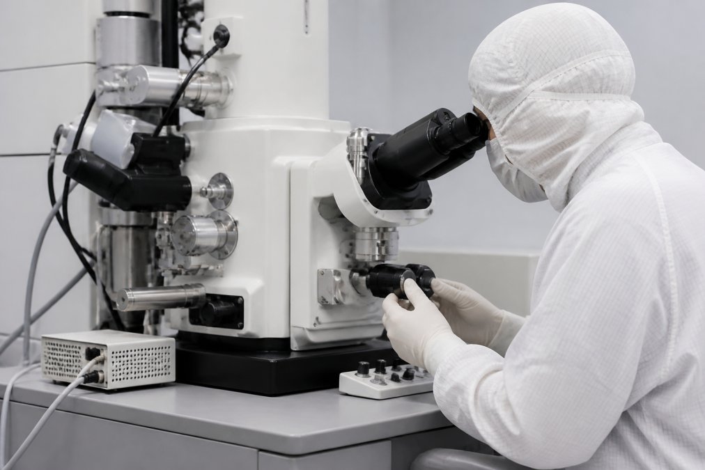
Professional illustration showing Close, SEM for particle detection methods
Scanning electron microscopy provides exceptional resolution for sub-10nm particle visualization, typically achieving 1-2nm resolution under optimal conditions. The SEM uses a focused electron beam to scan across a sample surface, with secondary and backscattered electrons creating high-contrast images that reveal particle morphology in detail.
Most modern SEMs include energy-dispersive X-ray spectroscopy (EDS) detectors that identify elemental composition at individual particle locations. This dual capability, seeing both morphology and composition simultaneously, provides information that optical methods cannot match.
However, SEM has practical limitations. Sample preparation is time-consuming and can introduce artifacts. The technique requires high vacuum conditions, limiting analysis of volatile or moisture-sensitive samples. Most critically, SEM is inherently low-throughput; you examine selected particles on a prepared slide, not the full population in a sample. For real-time contamination monitoring, SEM is too slow.
Transmission electron microscopy achieves sub-nanometer resolution by transmitting electrons through thin samples rather than reflecting them from surfaces. TEM can visualize individual atoms and reveals internal particle structure, crystallinity, and lattice defects.
For sub-10nm particle analysis, TEM excels at characterizing nanoparticles in the 1-10nm range with unprecedented clarity. Unlike SEM, which shows surface features, TEM reveals internal structure and whether a nanoparticle is crystalline or amorphous.
The trade-offs are severe. TEM requires extremely thin samples (typically 50-100nm thickness), demanding sophisticated sample preparation techniques. The instrument costs millions of dollars and requires specialized training. TEM provides no information about particle size distribution in your actual sample; you’re examining a tiny, artificially prepared slice that may not be representative.
TEM is the right choice when you need to understand internal structure and properties of nanoparticles, particularly for research applications or failure analysis. It’s not practical for routine contamination monitoring in manufacturing environments.
Condensation particle counters represent a fundamentally different approach to sub-10nm detection. Rather than visualizing individual particles, CPCs count and size particles by growing them into larger droplets that can be detected optically. This technique enables real-time, high-throughput particle counting with excellent sensitivity down to the 2.5nm range.
A CPC works by introducing sample air containing nanoparticles into a saturated vapor chamber, typically using butanol or diethylene glycol as the working fluid. As the sample cools, the vapor becomes supersaturated, and nanoparticles act as nucleation sites for condensation. The particles grow into much larger droplets (typically 10-15 micrometers) that scatter light efficiently and can be counted optically.
The critical advantage of CPC technology is sensitivity. Particles as small as 2.5nm can nucleate condensation and be counted, making CPCs far more sensitive than optical particle counters that rely on light scattering from the original particle size.
However, CPC technology has important limitations. First, the technique counts particles but provides only limited size information. A CPC can tell you how many particles are in your sample, but determining whether those particles are 3nm or 8nm requires additional instrumentation. Second, all particles above the CPC’s detection threshold grow and are counted equally, losing the ability to distinguish between different particle populations by size unless combined with other techniques. Third, CPC operation requires careful attention to working fluid management, temperature stability, and calibration.
The real power of CPC technology emerges when combined with a differential mobility particle sizer (DMPS). A DMPS classifies particles by electrical mobility, essentially their size, by passing them through an electrical field that separates them into different size bins. The CPC then counts particles in each bin, providing a complete size distribution.
A DMPS-CPC system can characterize ultrafine aerosol populations with size resolution as fine as 5nm steps across the range from approximately 3nm to 1 micrometer. This combination is the standard approach for aerosol research, ambient air quality monitoring, and industrial hygiene assessments.
For semiconductor fabs and cleanroom facilities, DMPS-CPC systems provide real-time monitoring of ultrafine particle concentrations and size distributions. Unlike grab-sample methods that give you a snapshot at one moment in time, a DMPS-CPC continuously streams data showing how particle concentrations change throughout the day and whether contamination events are occurring.
Watch Out A common mistake is assuming that DMPS-CPC data directly represents the particle population you care about. The system measures electrical mobility, which correlates with size but isn’t identical to geometric size. Particles with unusual shapes or electrical properties may be misclassified. Always validate DMPS-CPC findings with complementary techniques like TEM or SEM when making critical manufacturing decisions.
Dynamic light scattering measures particle size by analyzing how particles in a liquid suspension scatter laser light as they move randomly through Brownian motion. The technique is fast, requires minimal sample preparation, and works well for particles in the 2nm to several micrometer range.
When a laser beam passes through a particle suspension, particles scatter light in all directions. Because particles move randomly due to thermal energy, the intensity of scattered light fluctuates over time. Larger particles move more slowly and create slower intensity fluctuations; smaller particles move faster and create faster fluctuations. By analyzing the autocorrelation of the scattered light intensity over time, DLS software calculates the particle size distribution.
The major advantage of DLS is speed and simplicity. A measurement takes seconds to minutes, requires only a small sample volume (typically 10-50 microliters), and demands no sample preparation beyond basic dilution. For biopharmaceutical applications where you need to characterize nanoparticle suspensions, liposomes, polymeric nanoparticles, or protein aggregates, DLS is often the first-choice method.
However, DLS has significant limitations for sub-10nm work. The technique assumes spherical particles; non-spherical particles are misclassified. DLS is sensitive to aggregation and can misinterpret aggregates as larger single particles. Most critically, DLS provides intensity-weighted size distributions, which biases results toward larger particles. A sample containing mostly 5nm particles with a small fraction of 50nm aggregates will appear dominated by the larger particles in DLS data, even though they represent a tiny fraction by number.
For sub-10nm characterization, DLS works best as a screening tool or as part of a multi-technique approach. Combine DLS with transmission electron microscopy or single particle ICP-MS for more reliable characterization of nanoparticle populations below 10nm.
Single particle inductively coupled plasma mass spectrometry detects individual nanoparticles by measuring the elemental composition of each particle as it enters an ICP-MS instrument. This method is particularly valuable for engineered nanoparticles containing metals or metalloids, silver nanoparticles, gold nanoparticles, titanium dioxide, zinc oxide, and similar materials.
In SP-ICP-MS, a dilute nanoparticle suspension is nebulized into the ICP-MS at a rate such that individual particles enter the plasma one at a time. Each particle is ionized and its elemental composition is measured via mass spectrometry. The instrument detects a distinct signal for each particle, allowing you to count particles and measure their elemental mass simultaneously.
The size of the mass spectrometry signal correlates directly with the mass of the element in each particle. For spherical nanoparticles of uniform composition, this mass measurement can be converted to particle size. More importantly, SP-ICP-MS tells you exactly how much of the target element (silver, gold, titanium, etc.) is in each particle.
SP-ICP-MS excels at detecting engineered nanoparticles in complex matrices. A pharmaceutical sample containing trace amounts of silver nanoparticles from a manufacturing process, a water sample containing titanium dioxide nanoparticles from sunscreen, or an environmental sample containing engineered gold nanoparticles from nanotechnology research, SP-ICP-MS can identify and characterize these materials even when present at very low concentrations.
However, SP-ICP-MS only works for nanoparticles containing elements detectable by mass spectrometry. Organic polymers, carbon-based nanoparticles, and silica particles cannot be characterized. The technique requires sophisticated instrumentation and expert operation. For biopharmaceutical applications involving engineered metal nanoparticles or metal contamination analysis, SP-ICP-MS is uniquely powerful.
The most reliable sub-10nm particle detection strategies combine multiple techniques, each contributing different information about the particle population. No single method captures all relevant properties; instead, a tiered approach uses fast screening methods, confirmatory techniques, and specialized characterization tools in a logical workflow.
A typical workflow for comprehensive nanoparticle characterization might begin with dynamic light scattering or optical particle counting to establish that a particle population exists and estimate its approximate size range. This screening step is fast and inexpensive. If DLS indicates particles in the 5-20nm range, you then move to confirmatory techniques like transmission electron microscopy or SEM to visualize the particles directly and assess their morphology and aggregation state.
For elemental analysis, single particle ICP-MS adds information about composition if the particles contain detectable elements. For aerosol applications, DMPS-CPC characterization provides real-time size distribution data with excellent resolution. The specific combination depends on your application and what questions you’re trying to answer.
Applied Physics works with cleanroom managers, process engineers, and quality assurance teams to design workflows that match their specific needs. A semiconductor fab pursuing sub-10nm node production requires different metrology than a biopharmaceutical compounding pharmacy, which requires different instrumentation than a nanotechnology research lab.
Semiconductor fabrication at advanced nodes depends critically on sub-10nm particle detection and control. Particles in this size range can cause defects that reduce yield and compromise product reliability. Process engineers need not just detection capability, but calibration standards that verify their instruments are performing correctly.
NIST-traceable calibration wafer standards provide reference particles of known size and composition that allow you to validate your SEM, TEM, or other metrology tools. Without proper calibration, you cannot trust your measurement results. Applied Physics provides calibration wafer standards specifically designed for semiconductor metrology applications, enabling facilities to validate their detection instruments against traceable references.
Best For Semiconductor fabs pursuing 5nm and below node production, and research institutions developing advanced nanomaterials requiring verified sub-10nm detection capability.
Sub-10nm particle detection introduces challenges that don’t exist at larger scales. Understanding these challenges helps you interpret results correctly and avoid costly mistakes in process control decisions.
One of the most common artifacts in sub-10nm work is misidentification of aggregates as single particles. When nanoparticles aggregate, they can appear as larger single particles in some techniques. DLS is particularly susceptible to this error. A sample containing mostly 5nm particles with some 15nm aggregates will appear dominated by the larger particles in intensity-weighted DLS data. SEM can visually distinguish aggregates from single particles, but only if you examine enough particles to establish statistical significance.
Sample preparation introduces another class of artifacts. Drying samples for SEM or TEM can cause particles to move, aggregate, or distort. Staining or coating samples for electron microscopy can obscure fine surface features or change apparent particle size. Diluting samples for DLS or aerosol methods can introduce new contamination or cause particles to aggregate differently than in the original sample.
Software interpretation of raw data is often where errors occur. DMPS-CPC systems generate size distribution data based on electrical mobility calculations that assume spherical, singly-charged particles. Real-world particles may be non-spherical or multiply-charged, leading to systematic size classification errors. DLS software uses mathematical inversion algorithms to convert autocorrelation functions into size distributions; different algorithms can produce different results from the same raw data.
Watch Out Always examine raw data, not just software-generated summaries. A DMPS-CPC size distribution plot might show a single peak that looks clean and interpretable, but the raw count data might reveal that 95% of particles are at the detection limit with only a few particles in the main peak. This situation demands different interpretation than a distribution where thousands of particles populate the main peak.
The cost of sub-10nm detection spans multiple dimensions: instrument acquisition, maintenance and calibration, training and expertise, sample preparation, and analysis time. The lowest-cost option is rarely the best choice.
Optical particle counters cost tens of thousands of dollars and provide rapid, continuous monitoring, excellent for real-time contamination tracking in cleanrooms. However, they cannot detect below approximately 0.5 micrometers. Adding a DMPS-CPC system costs substantially more but enables real-time ultrafine aerosol monitoring. Electron microscopy systems cost hundreds of thousands of dollars and require expert operation, but provide unmatched morphological detail. Single particle ICP-MS systems are expensive and require sophisticated chemistry expertise, but provide unique elemental analysis capabilities.
The right choice depends on your facility’s operational needs and regulatory requirements. Consider total cost of ownership, not just purchase price. A cheaper instrument that requires frequent calibration, produces unreliable data, or demands extensive expertise may cost far more over its lifetime than a more expensive but robust system.
Cleanroom managers and quality assurance officers in biopharmaceutical facilities face specific regulatory and operational constraints that shape how sub-10nm detection is implemented.
USP <797> and <800> standards require pharmaceutical compounding facilities to control particulate matter in injectable preparations and hazardous drugs. While these standards focus primarily on particles larger than 10 micrometers, the regulatory expectation is that facilities understand and control their contamination sources, including potential ultrafine particle generation.
A GMP-validated particle detection system requires documented procedures for instrument calibration, maintenance, data recording, and corrective action. The system must be qualified for your specific application; simply purchasing an instrument is insufficient. Qualification involves installing the system, verifying it works as specified, and demonstrating it produces reproducible, accurate results under your facility’s actual operating conditions.
For sub-10nm detection in compounding pharmacies, a practical approach often combines optical particle counting for routine cleanroom monitoring with periodic SEM analysis of specific samples when particulate matter investigations are needed. This tiered approach provides continuous monitoring at reasonable cost while maintaining the capability to investigate specific contamination events in detail.
All particle detection instruments drift out of calibration over time. Environmental factors like temperature and humidity, instrument aging, and normal wear on optical or electronic components all contribute to measurement drift. Regular calibration against NIST-traceable standards is essential for maintaining measurement integrity.
For optical particle counters, calibration typically uses polystyrene latex (PSL) particles of known size and concentration. For electron microscopy, calibration uses standard reference samples or calibration grids. For aerosol systems like DMPS-CPC, calibration involves generating particles of known size and verifying that the system counts them correctly.
Maintenance schedules depend on the specific instrument and your facility’s operating conditions. A particle counter in a heavily contaminated environment requires more frequent maintenance than one in a clean environment. Most manufacturers provide maintenance recommendations; following them is essential for sustained accuracy.
Quality assurance for sub-10nm detection includes periodic inter-laboratory comparisons when possible, participation in proficiency testing programs if available for your specific application, and regular review of measurement trends. If your SEM suddenly starts reporting particles as 20% larger than historical data, that’s a calibration drift signal that demands investigation.
USP <797> and <800> standards for pharmaceutical compounding provide the authoritative requirements for sterile compounding facilities. Compliance requires not just having detection capability, but documenting that your detection systems are validated, calibrated, and operated correctly.
Contamination control in critical manufacturing environments depends on detecting and characterizing particles at scales where conventional tools fail. The sub-10nm particle detection methods available today, from optical microscopy and electron microscopy to aerosol counters and elemental analysis techniques, each offer different capabilities, trade-offs, and practical constraints.
The right choice for your facility depends on your specific application: whether you’re validating cleanroom airflow patterns for GMP compliance, qualifying calibration wafer standards for semiconductor metrology, ensuring particle safety in injectable biopharmaceuticals, or characterizing engineered nanoparticles in research. No single technique answers all questions. The most reliable approach combines multiple methods in a logical workflow that screens, confirms, and characterizes particle populations with appropriate depth for your decision-making needs.
Applied Physics has supported precision contamination control and semiconductor metrology across three decades of advancing manufacturing standards. Our calibration wafer standards enable semiconductor fabs to validate their sub-10nm detection instruments against NIST-traceable references, ensuring measurement integrity for critical process control decisions. Contact us to discuss how a comprehensive detection and validation strategy can support your facility’s operational excellence and regulatory compliance.
Sub-10nm particle detection faces several critical challenges: particles at this scale interact weakly with light, making optical methods unreliable; Brownian motion causes rapid diffusion, complicating measurement stability; and instrumental detection limits often approach the size of the particles themselves. Additionally, distinguishing true nanoparticles from measurement noise and aggregates requires sophisticated data interpretation and software capabilities. Sample preparation, calibration accuracy, and maintaining controlled conditions during analysis add complexity to achieving reliable results.
A CPC works by saturating particles with a condensable vapor (typically butanol), then cooling the sample to create supersaturation. This forces vapor to condense onto nanoparticles, enlarging them to optically detectable sizes (typically 1-2 micrometers). Once enlarged, an optical detector counts individual particles. CPCs can detect particles as small as 2.5nm, making them ideal for aerosol characterization in cleanrooms. When paired with a Differential Mobility Particle Sizer (DMPS), CPCs provide size-resolved measurement data essential for validating airflow patterns and contamination control.
TEM transmits electrons through ultra-thin samples, providing atomic-scale resolution (often sub-1nm) and detailed morphology information, making it ideal for characterizing nanoparticle structure, crystallinity, and internal composition. SEM scans a focused electron beam across the sample surface, offering excellent surface morphology and elemental analysis via energy-dispersive X-ray spectroscopy (EDS), but with lower resolution than TEM. TEM requires extensive sample preparation and expertise; SEM is faster and more accessible. For sub-10nm detection, TEM delivers superior precision, while SEM excels at rapid screening and elemental identification.
SP-ICP-MS ionizes individual nanoparticles and measures their elemental composition and mass with high sensitivity, allowing detection of particles as small as 5-10nm depending on the element. Unlike bulk ICP-MS, which analyzes dissolved samples, SP-ICP-MS preserves particle identity, enabling determination of particle size distribution, elemental composition, and number concentration in a single analysis. This technique is particularly valuable for biopharmaceutical applications, environmental monitoring, and semiconductor metrology where understanding both the physical and chemical properties of nanoparticles is critical for process control.

Enter your details below to save your shopping cart for later. And, who knows, maybe we will even send you a sweet discount code :)
Allow notifications to get real-time updates about your shopping cart and who knows, you may even receive a sweet discount code 😊