
Applied Physics · Precision technologies since 1992
Request Quote

Next-Gen Metrology Challenges for Sub-5nm Semiconductor Nodes
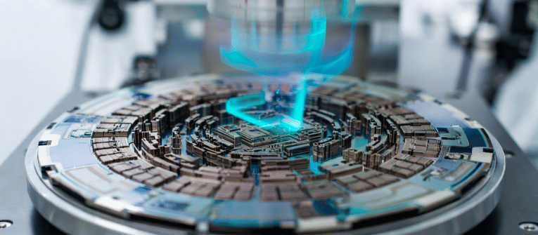
Metrology machine inspecting a precision microchip wafer with advanced laser measurement technology

Semiconductor manufacturing is pushing physical limits. As fabrication drops below the 5-nanometer (nm) threshold, reaching 3nm and 2nm nodes, the methods used to measure and inspect silicon wafers must adapt. Metrology, the science of measurement, is facing severe technical bottlenecks. Accurately detecting defects and measuring critical dimensions (CD) at this scale requires entirely new approaches […]

You were not leaving your cart just like that, right?

You were not leaving your cart just like that, right?

Enter your details below to save your shopping cart for later. And, who knows, maybe we will even send you a sweet discount code :)

Want to receive personalized offers?

Allow notifications to get real-time updates about your shopping cart and who knows, you may even receive a sweet discount code 😊

Maybe later