
Advanced Metrology for Sub-10nm Defect Classification on Wafers
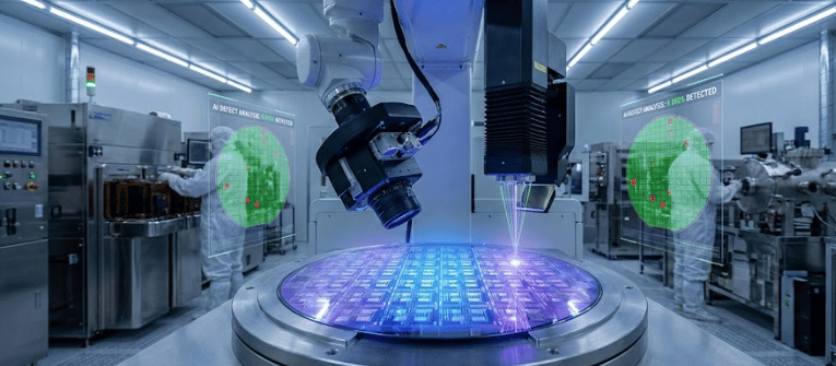
The semiconductor industry’s march toward the angstrom era has fundamentally altered the physics of manufacturing. As fabs transition to 5nm, 3nm, and 2nm nodes, the margin for error has effectively vanished. In this regime, a defect the size of a single DNA strand can render a chip useless. For yield engineers, the challenge is no […]
