
Applied Physics · Precision technologies since 1992
Request Quote

Advanced Metrology for Sub-10nm Defect Classification on Wafers
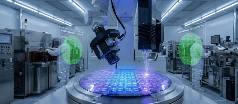
Cleanroom wafer inspection with robotic laser and camera scanning microchips, technicians monitoring holographic defect-analysis displays

The semiconductor industry’s march toward the angstrom era has fundamentally altered the physics of manufacturing. As fabs transition to 5nm, 3nm, and 2nm nodes, the margin for error has effectively vanished. In this regime, a defect the size of a single DNA strand can render a chip useless. For yield engineers, the challenge is no […]

You were not leaving your cart just like that, right?

You were not leaving your cart just like that, right?

Enter your details below to save your shopping cart for later. And, who knows, maybe we will even send you a sweet discount code :)

Want to receive personalized offers?

Allow notifications to get real-time updates about your shopping cart and who knows, you may even receive a sweet discount code 😊

Maybe later