
Achieving Zero-Residue Airflow Visualization with AP35 Technology
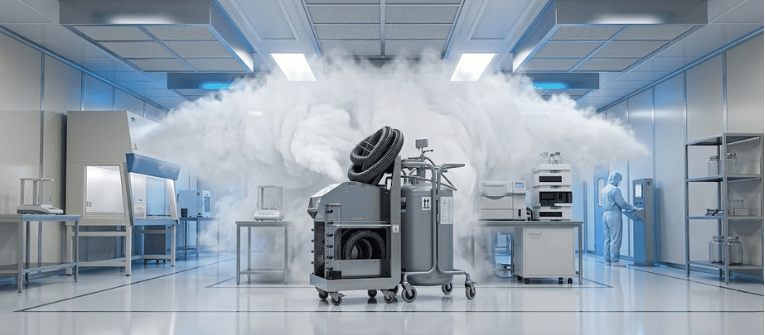
Cleanroom environments, such as those in semiconductor manufacturing and pharmaceutical production, require extremely precise airflow mapping without introducing any contamination. Our AP35 Ultrapure Fogger handles this exact requirement. The system operates using Liquid Nitrogen (LN2) and high‑purity water, generating a highly dense, neutrally buoyant fog. This allows facilities to perform full 3D airflow modeling, identify dead zones, and verify cleanroom dynamics, […]
How Advanced Wafer Calibration Standards Minimize Defects in Next-Gen Semiconductor Fabrication
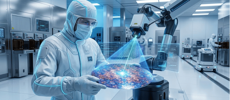
In the hyper-competitive world of semiconductor manufacturing, the difference between a high-yield production run and a multi-million dollar loss is measured in nanometers. As the industry pushes the boundaries of Moore’s Law, moving into sub-5nm process nodes, the size of a killer defect has shrunk to a point where even the most advanced inspection tools […]
Managing Molecular Contamination in Extreme Ultraviolet (EUV) Pods
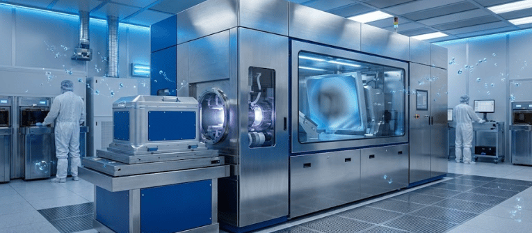
As semiconductor manufacturing pushes beyond the 5 nm logic node, Extreme Ultraviolet (EUV) lithography has become the undisputed engine of modern chipmaking. However, operating at a wavelength of 13.5 nm introduces unprecedented physical and chemical sensitivities. Among the most complex hurdles in maximizing EUV uptime and yield is molecular contamination, specifically within the EUV reticle […]
Optimizing Argon Ion Etching for Surface Pre-Treatment
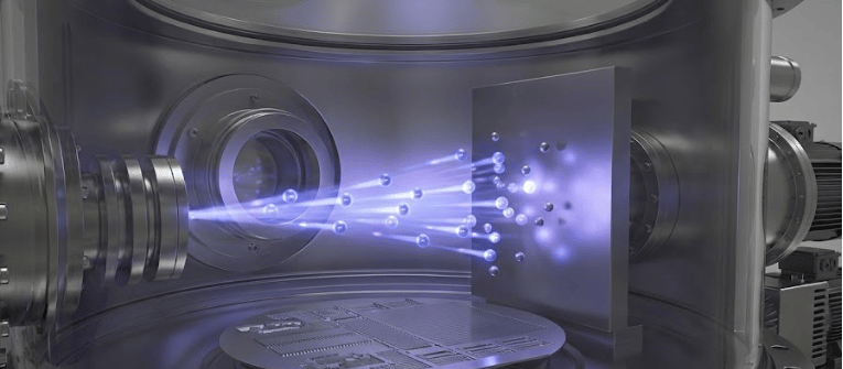
The world of precision manufacturing, from semiconductor fabrication to advanced aerospace coatings, the quality of a surface determines the success of the entire project. Argon Ion Etching (AIE) has emerged as the gold standard for high-fidelity surface pre-treatment. This article explores the technical nuances of optimizing Argon Ion Etching to ensure maximum adhesion, purity, and […]
How to Choose the Best Calibration Wafer Standard for Optical Inspection Tools
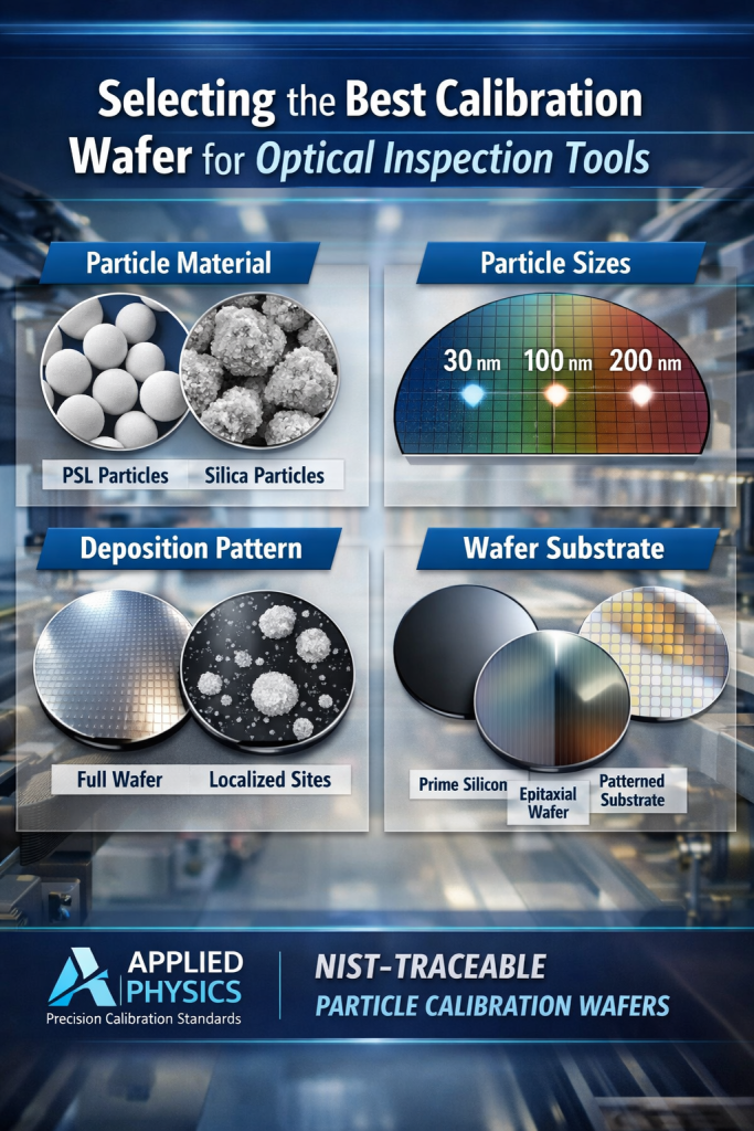
In modern semiconductor manufacturing, optical inspection tools are only as reliable as the standards used to calibrate them. As critical dimension control tightens and defect budgets shrink, selecting the right calibration wafer standard is no longer a formality—it is a foundational requirement for process control, tool matching, and regulatory confidence. At Applied Physics., we work […]
Wafer Thickness: The Ultimate Guide to Getting It Right

Introduction Wafer thickness plays a crucial role in semiconductor manufacturing, as it directly impacts the performance and quality of the final semiconductor devices. The thickness of the wafer determines the electrical and mechanical properties of the semiconductor, making it a critical parameter in the production process. A uniform wafer thickness is essential for ensuring consistent […]
10 Expert Tips to Achieve Wafer Standard Perfection
Introduction The wafer standard refers to a set of specifications and criteria that govern the production and quality of semiconductor wafers, which are essential components in the manufacturing of integrated circuits. These standards encompass various parameters, including thickness, diameter, surface roughness, and crystal orientation. The primary goal of adhering to these standards is to ensure […]
What is Photolithography? The Core of Semiconductor Design
Photolithography is a vital process in semiconductor manufacturing, involving the use of light to transfer patterns onto a substrate, typically a silicon wafer. This process is essential for creating the intricate patterns and structures that form the foundation of semiconductor devices, such as integrated circuits (ICs) and microprocessors. The photolithography process requires advanced equipment and […]
Why Semiconductor Manufacturing Needs Ultra-Pure Water
Semiconductor manufacturing is a highly intricate and precise process that necessitates the use of ultra-pure water to guarantee the quality and reliability of the final product. In this process, ultra-pure water serves as a vital component in various stages, including cleaning, rinsing, etching, and photoresist development. The purity of the water used in these stages […]
