
Are High-End Semiconductor Wafer Calibration Standards Worth the Investment for Improving Node Transition Yields?
Learn when high-end wafer calibration standards justify their cost during semiconductor node transitions, yield ramp, SSIS matching, and particle sensitivity tuning.
Next-Gen Metrology Challenges for Sub-5nm Semiconductor Nodes
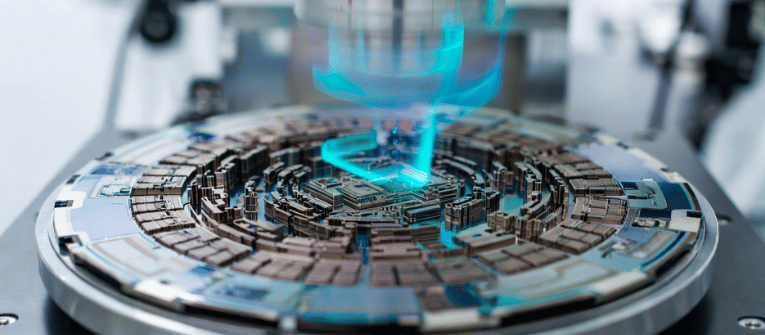
Semiconductor manufacturing is pushing physical limits. As fabrication drops below the 5-nanometer (nm) threshold, reaching 3nm and 2nm nodes, the methods used to measure and inspect silicon wafers must adapt. Metrology, the science of measurement, is facing severe technical bottlenecks. Accurately detecting defects and measuring critical dimensions (CD) at this scale requires entirely new approaches […]
Impact of Particle Contamination on Next-Gen Chip Manufacturing

The semiconductor industry is currently navigating a transition where the margin for error has effectively vanished. As fabrication facilities (fabs) move toward 3nm and 2nm process nodes, the killer defect is no longer a visible speck of dust; it is a microscopic particle often smaller than the wavelength of visible light. In this environment, a […]
Silica vs. PSL Spheres: Why Silica Particles Are Better in High‑Temperature
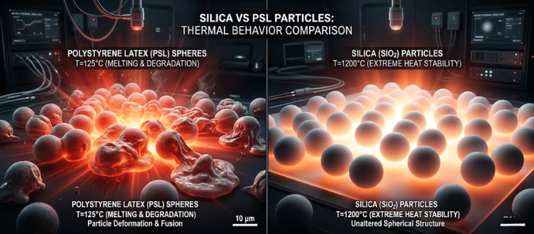
In the world of precision metrology and cleanroom validation, accuracy is non-negotiable. For decades, Polystyrene Latex (PSL) spheres have been the industry standard for calibrating particle counters and inspecting wafers. However, as semiconductor and pharmaceutical manufacturing processes push into higher temperature ranges, the limitations of PSL have become apparent. Enter Silica (SiO2) particles. While both […]
Scaling the 1nm Frontier: Next-Gen Metrology Standards for AI-Centric Chip Manufacturing in 2026
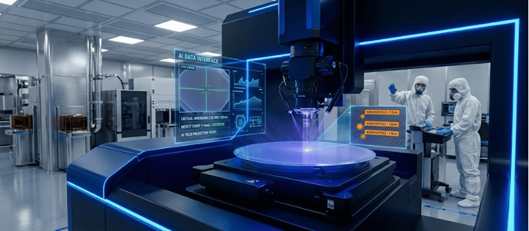
The semiconductor industry has officially entered the era of the Angstrom gap. As of 2026, the push toward 1nm and sub-1nm nodes is no longer a roadmap projection; it is a production reality driven by the insatiable demand for AI-centric high-performance computing (HPC). However, shrinking transistor dimensions to the atomic scale introduces a critical bottleneck: […]
Advanced Metrology for Sub-10nm Defect Classification on Wafers
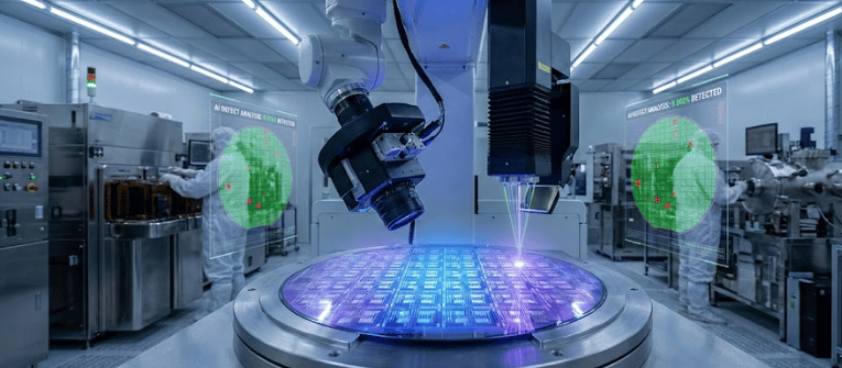
The semiconductor industry’s march toward the angstrom era has fundamentally altered the physics of manufacturing. As fabs transition to 5nm, 3nm, and 2nm nodes, the margin for error has effectively vanished. In this regime, a defect the size of a single DNA strand can render a chip useless. For yield engineers, the challenge is no […]
What Are the Top Calibration Wafer Standards Used in Semiconductor Manufacturing?
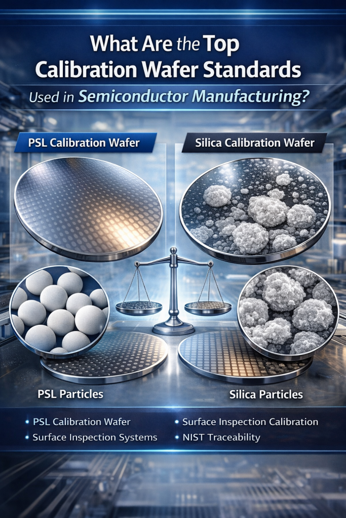
Calibration wafer standards are a foundational component of semiconductor metrology, enabling accurate contamination monitoring, inspection tool calibration, and long-term process control in advanced IC fabs. As device geometries continue to scale below 5 nm, inspection tools must be calibrated using reference wafers that provide repeatable, traceable, and process-relevant particle characteristics. The most widely used calibration […]
Which Suppliers Offer Quick Shipping for Calibration Wafer Standards?

Fast access to calibration wafer standards is critical in semiconductor manufacturing, where inspection tool downtime, tool qualification windows, and process changes can directly impact yield and production schedules. Calibration wafer standards—also commonly referred to as PSL wafer standards or particle calibration wafers—are used exclusively for particle size calibration of wafer inspection systems in IC manufacturing […]
How to Choose the Best Calibration Wafer Standard for Optical Inspection Tools
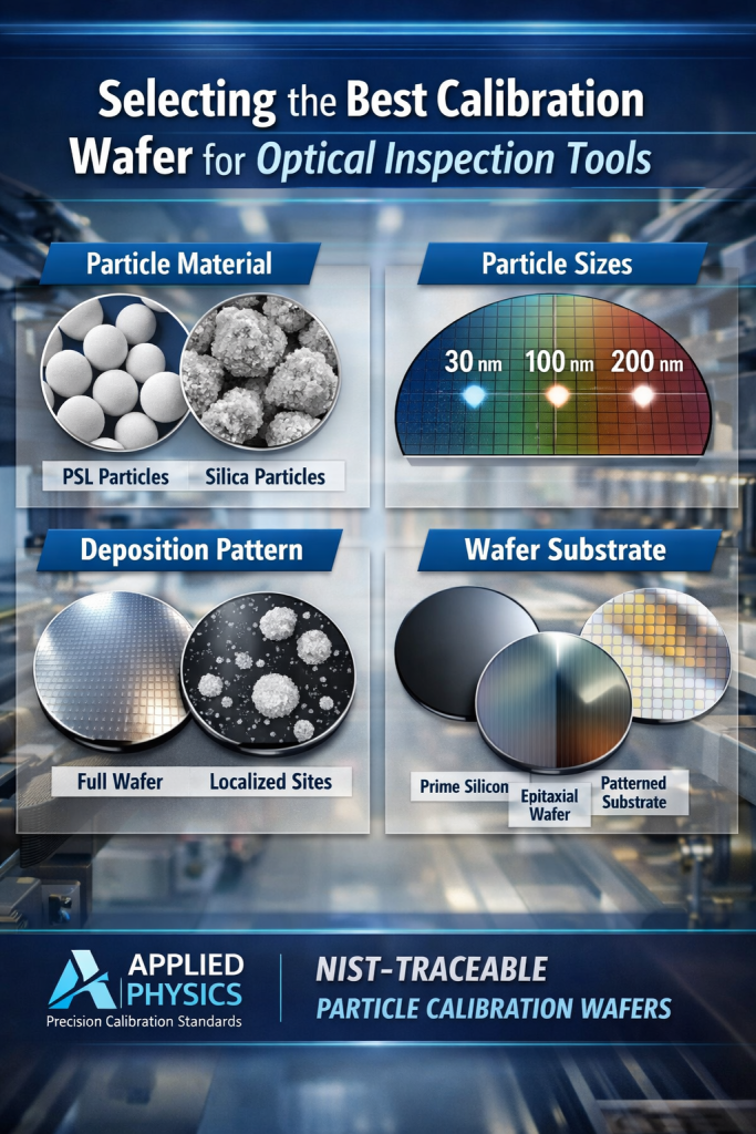
In modern semiconductor manufacturing, optical inspection tools are only as reliable as the standards used to calibrate them. As critical dimension control tightens and defect budgets shrink, selecting the right calibration wafer standard is no longer a formality—it is a foundational requirement for process control, tool matching, and regulatory confidence. At Applied Physics., we work […]
Why SSIS Tools Must Be Calibrated to NIST-Traceable Particle Size Standards
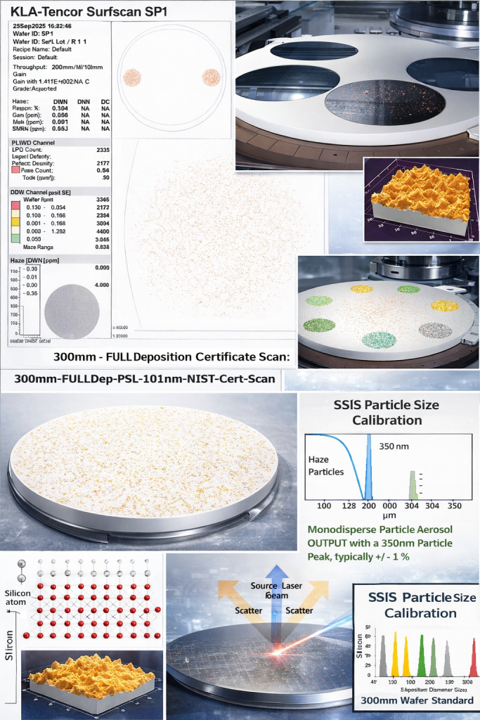
SSIS tools (Surface Scanning Inspection Systems) must be calibrated to NIST-traceable particle size standards to ensure particle sizing is consistent, comparable, and actionable across tools, fabs, and time. When particle size data is accurate and standardized, contamination control teams can identify sources faster, reduce false alarms, improve tool matching, and protect yield—especially at advanced nodes […]
