
Precision Metrology for Measuring Surface Energy of Treated Wafers
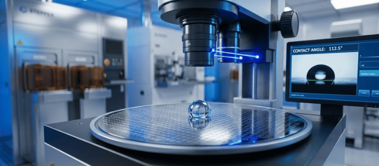
In modern semiconductor manufacturing, the margin for error is measured in nanometers. As devices shrink and architectures become more complex, the surface conditions of silicon wafers dictate the success or failure of subsequent processing steps. One of the most critical, yet sometimes overlooked, parameters is surface energy. Understanding and controlling the surface energy of treated […]
