
Next-Gen Metrology Challenges for Sub-5nm Semiconductor Nodes
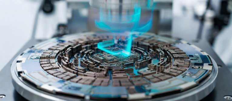
Semiconductor manufacturing is pushing physical limits. As fabrication drops below the 5-nanometer (nm) threshold, reaching 3nm and 2nm nodes, the methods used to measure and inspect silicon wafers must adapt. Metrology, the science of measurement, is facing severe technical bottlenecks. Accurately detecting defects and measuring critical dimensions (CD) at this scale requires entirely new approaches […]
