
Beyond PSL: The Growing Importance of Silica Wafer Standards in Sub-20nm Node Metrology
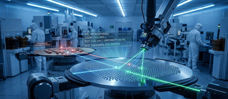
As the semiconductor industry aggressively scales toward 7nm, 5nm, and even smaller process nodes, the precision required for contamination monitoring has reached an inflection point. For decades, Polystyrene Latex (PSL) microspheres have served as the industry gold standard for calibrating Scanning Surface Inspection Systems (SSIS). However, as particle size detection requirements drop below the 20nm […]
Which Suppliers Offer Quick Shipping for Calibration Wafer Standards?

Fast access to calibration wafer standards is critical in semiconductor manufacturing, where inspection tool downtime, tool qualification windows, and process changes can directly impact yield and production schedules. Calibration wafer standards—also commonly referred to as PSL wafer standards or particle calibration wafers—are used exclusively for particle size calibration of wafer inspection systems in IC manufacturing […]
How to Choose the Best Calibration Wafer Standard for Optical Inspection Tools
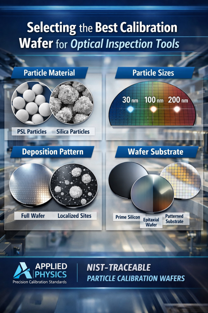
In modern semiconductor manufacturing, optical inspection tools are only as reliable as the standards used to calibrate them. As critical dimension control tightens and defect budgets shrink, selecting the right calibration wafer standard is no longer a formality—it is a foundational requirement for process control, tool matching, and regulatory confidence. At Applied Physics., we work […]
Why SSIS Tools Must Be Calibrated to NIST-Traceable Particle Size Standards
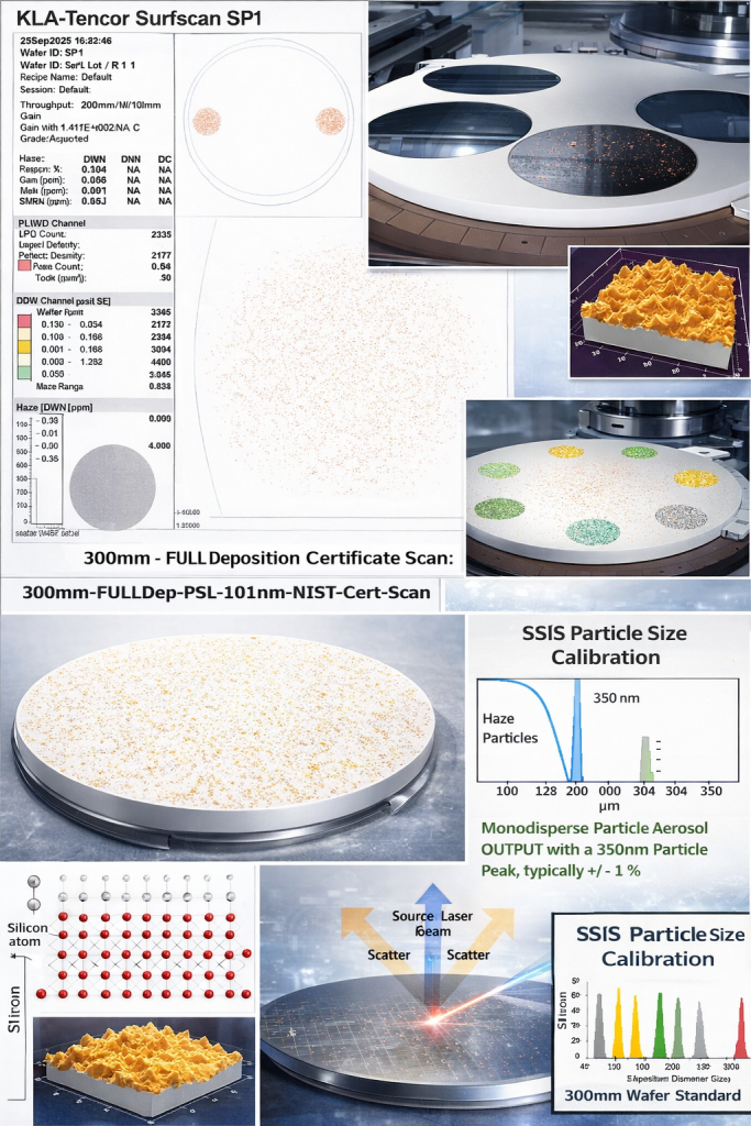
SSIS tools (Surface Scanning Inspection Systems) must be calibrated to NIST-traceable particle size standards to ensure particle sizing is consistent, comparable, and actionable across tools, fabs, and time. When particle size data is accurate and standardized, contamination control teams can identify sources faster, reduce false alarms, improve tool matching, and protect yield—especially at advanced nodes […]
