
What Are the Top Calibration Wafer Standards Used in Semiconductor Manufacturing?
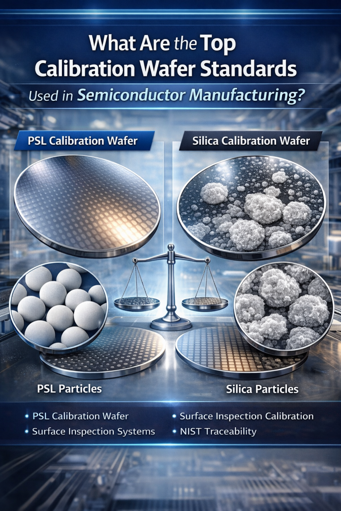
Calibration wafer standards are a foundational component of semiconductor metrology, enabling accurate contamination monitoring, inspection tool calibration, and long-term process control in advanced IC fabs. As device geometries continue to scale below 5 nm, inspection tools must be calibrated using reference wafers that provide repeatable, traceable, and process-relevant particle characteristics. The most widely used calibration […]
Particle Contamination on Silicon Wafers and Film-Deposited Wafers: What IC Fabs Must Know
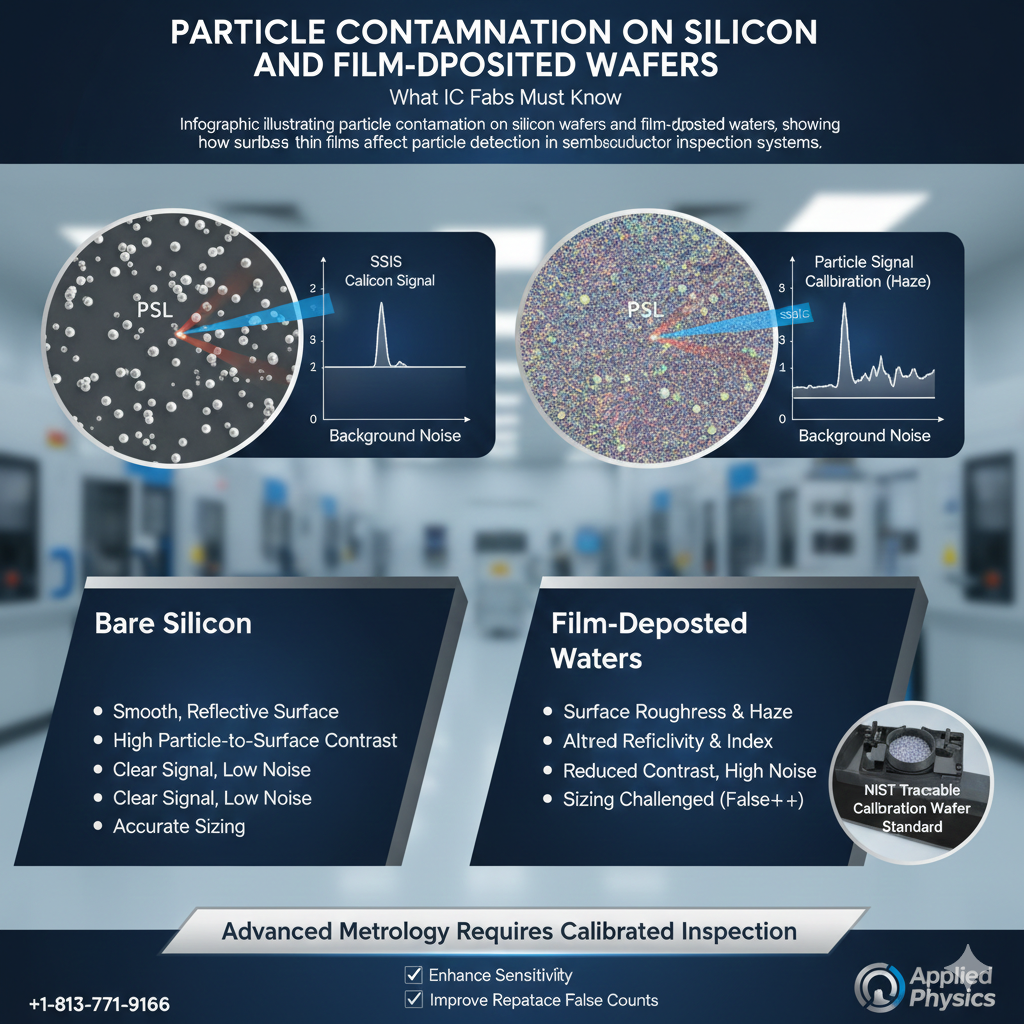
Particle contamination on silicon and film-deposited wafers occurs when unwanted nano- or micro-scale particles settle on wafer surfaces during semiconductor processing. These particles can disrupt lithography, seed defects in deposited films, and reduce yield—especially at advanced process nodes. Effective contamination control depends on accurate inspection, proper tool calibration, and an understanding of how wafer surfaces […]
