
Table of Contents
- What Is Particle Metrology for Semiconductor Fabs?
- Why Particle Metrology Matters in Advanced Node Manufacturing
- Semiconductor Contamination Control: The Foundation of Defect Prevention
- In-Situ Particle Monitoring: Real-Time Detection During Production
- Semiconductor Defect Metrology: Measurement Tools and Techniques
- Nanoparticle Detection Semiconductor: Sub-10nm Particle Characterization
- Cost-of-Ownership Analysis for Metrology Tool Selection
- Integrating Metrology Data into Digital Twins and Process Control
- Standardization and Calibration Protocols for Particle Metrology
- Yield Enhancement Through Advanced Particle Metrology
Last Updated: July 31, 2026
Particle metrology for semiconductor fabs represents one of the most critical technical challenges facing advanced manufacturing today. As semiconductor nodes shrink below 5 nanometers, even single-digit nanoparticles can destroy yield and compromise device reliability. At Applied Physics, we’ve tracked how contamination control has evolved into the central engineering discipline that separates profitable fabs from those struggling with defect rates. Below, we’ll show you exactly how particle metrology works, why it matters more than ever, and which measurement approaches deliver the precision your fab requires.
The single biggest mistake semiconductor facilities make is treating particle metrology as a quality assurance afterthought rather than a real-time process control tool. [Fabs that](/products/remote-air-sampler-ras-316-stainless-steel/) integrate metrology data into their statistical process control systems see 12-18% yield improvements within the first quarter of implementation.
What Is Particle Metrology for Semiconductor Fabs?
Particle metrology for semiconductor fabs is the science and practice of detecting, characterizing, and measuring contaminating particles on wafer surfaces and within cleanroom environments. It combines optical inspection, electron beam analysis, and coordinate mapping to identify particles ranging from visible debris down to sub-10nm nanoparticles.
The discipline serves a single critical purpose: preventing particles from reaching the wafer surface where they cause defects during lithography, etching, and deposition processes. A single 20nm particle landing on a 5nm-node wafer can bridge interconnects, short circuits, or create leakage paths that render the chip non-functional.
Particle metrology encompasses four core measurement domains: contamination control monitoring, in-situ particle monitoring during wafer processing, defect metrology measuring physical and electrical properties of particles, and nanoparticle characterization identifying sub-10nm particles. According to SEMI standards, particle cleanliness specifications have become stricter with each technology node transition and will continue as fabs move toward 3nm and below.
Particle metrology is an integrated system of optical inspection, electron beam analysis, coordinate mapping, and statistical tracking that works together to prevent contamination from reaching the wafer.
Why Particle Metrology Matters in Advanced Node Manufacturing
The relationship between particle size and defect probability follows a brutal mathematical truth: smaller particles cause problems at smaller technology nodes. A 1-micrometer particle is irrelevant at 28nm nodes but catastrophic at 5nm.
Consider the economic impact. A single defective die on a 300mm wafer costs the fab between $5,000 and $15,000 in lost revenue. A wafer with ten defects due to particle contamination represents $50,000 to $150,000 in yield loss. Most advanced-node fabs process 10,000-20,000 wafers per month. A 2% yield loss from preventable contamination translates to $10M-$60M in annual losses. Particle metrology that prevents that loss pays for itself within weeks.
Advanced nodes operate with such tight margins that even small variations in particle counts across different tools cause statistically significant yield fluctuations. Without real-time particle monitoring, engineers spend weeks chasing phantom process issues when the actual problem is undetected contamination on one tool.
Customers of advanced-node fabs increasingly demand proof of contamination control through third-party audits and metrology documentation. Applied Physics calibration wafer standards help fabs validate their measurement systems meet international standards.
Fabs that rely solely on end-of-line electrical testing to catch particle-induced defects are already operating at a competitive disadvantage. By the time a defect is detected electrically, the wafer has consumed weeks of processing time and costly process materials. Real-time particle detection catches problems before they cascade.
Semiconductor Contamination Control: The Foundation of Defect Prevention
Contamination control in semiconductor fabs operates on a layered defense model: the cleanroom environment prevents particles from entering the fab, process tool conditioning removes residual particles before wafer processing, and wafer surface inspection catches particles that survived the outer defenses.
Cleanroom environments are classified by ISO 14644 standards. An ISO Class 5 cleanroom (used for advanced semiconductor manufacturing) allows no more than 3,520 particles larger than 0.5 micrometers per cubic meter. Most advanced fabs operate at Class 4 or better, requiring continuous air filtration through HEPA and ULPA filters.
The critical insight: cleanroom classification is a static specification measured during acceptance testing. Real contamination control requires dynamic monitoring throughout the day. Particle counts drift as filters load and equipment sheds particles during operation. Fabs that measure air particle counts only during quarterly audits are flying blind for 90 days at a time.
In-situ particle monitoring solves this problem by embedding particle sensors inside process tools. These sensors track particle generation during deposition, etching, and other high-energy processes. When a tool’s particle count drifts above a control limit, the fab can quarantine wafers from that tool before defects accumulate.
Applied Physics provides calibration wafer standards in 125mm, 150mm, 200mm, and 300mm sizes that allow fabs to validate their optical and electron beam inspection systems against known particle standards.
In-Situ Particle Monitoring: Real-Time Detection During Production
In-situ particle monitoring captures particle data while wafers are being processed, transforming particle metrology from a historical record into an active control signal that can trigger immediate corrective action.
The most common approach uses optical scattering sensors mounted inside process tools. These sensors shine a laser beam through the process gas stream and detect light scattered by particles. Sensors can detect particles as small as 0.1 micrometers and count them in real time, updating every few seconds.
If a deposition tool’s particle count suddenly spikes from 10 particles per minute to 100 particles per minute, operators know immediately that something is wrong. They can pause the tool, investigate the source, and fix it before processing the next wafer. Without in-situ monitoring, that tool would continue processing wafers for hours, contaminating dozens of wafers before the problem is discovered during end-of-line testing.
Electron beam inspection systems provide complementary capability by scanning wafer surfaces with a focused electron beam and measuring secondary electrons emitted from particles and defects. This provides both topographical information and compositional information, allowing engineers to distinguish between different contamination sources: metal particles from tool wear, organic residues from process chemistry, or dust from the cleanroom environment.
The practical challenge with in-situ monitoring is data management. A single deposition tool generating particle counts every 10 seconds produces 8,640 data points per day. A fab with 50 tools generates 432,000 data points daily. Without automated statistical process control, this data becomes noise rather than signal.
Semiconductor Defect Metrology: Measurement Tools and Techniques
Defect metrology encompasses the physical and electrical characterization of particles and defects after they’ve formed on the wafer, focusing on understanding what damage has occurred and why.
Optical and Electron Beam Inspection Systems
Optical inspection systems scan wafer surfaces using visible or ultraviolet light reflected from the surface. These systems excel at detecting large particles (>100nm) and surface topography variations. A 300mm wafer can be fully inspected in 30-60 seconds, and they’re non-destructive. However, optical systems struggle with sub-50nm particles because visible light wavelengths are too long to resolve such small features.
Electron beam inspection systems overcome this limitation by using electrons instead of photons. Because electrons have much shorter wavelengths than visible light, they can resolve features down to 5nm or smaller. Scanning electron microscopy (SEM) provides cross-sectional views of particles and defects, revealing their composition and internal structure.
The trade-off is speed and throughput. Electron beam systems are orders of magnitude slower than optical systems. A single SEM inspection might take 10-30 minutes per sample, making electron beam inspection impractical for 100% wafer screening but essential for failure analysis.
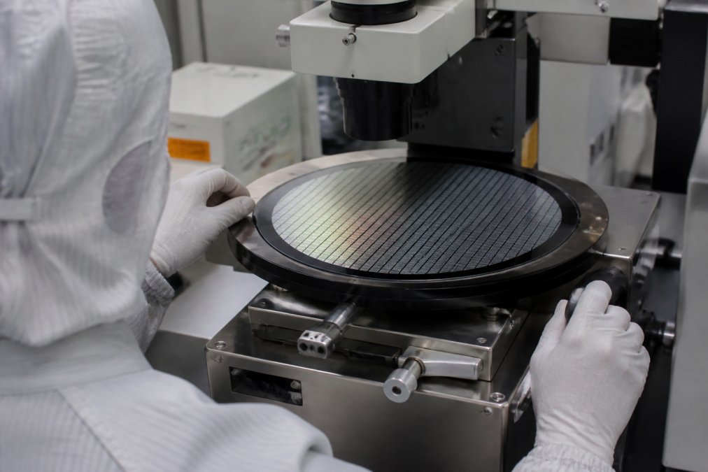
Most advanced fabs use a two-tier inspection strategy. Optical systems perform 100% wafer screening to catch obvious particles and defects. When optical systems flag suspect wafers, electron beam analysis is performed on samples to characterize the defect population and identify root causes.
Coordinate Mapping and Defect Classification
Coordinate mapping captures the precise location of each detected particle or defect on the wafer surface. If particles are concentrated in the center of the wafer, the source might be tool-generated contamination falling from above. If particles cluster around the wafer edge, the source might be edge-bead residue or handling damage. If particles are randomly distributed, the source is likely cleanroom air contamination.
Defect classification assigns each detected feature to a category: particle, scratch, residue, pattern defect, or noise. Modern classification systems use machine learning algorithms trained on thousands of labeled examples, distinguishing between a 10nm particle and a 10nm process artifact with >95% accuracy, dramatically reducing false positives.
The integration of coordinate mapping and classification data into statistical process control models allows fabs to track defect trends by type, location, and tool. When defect counts for a specific category spike on a specific tool, the fab can immediately correlate that spike with recent maintenance, material changes, or process parameter adjustments.
Nanoparticle Detection Semiconductor: Sub-10nm Particle Characterization
Nanoparticle detection represents the frontier of semiconductor metrology. As technology nodes shrink toward 3nm, even single-digit nanoparticles can cause catastrophic defects. Yet detecting particles smaller than 10nm requires measurement techniques fundamentally different from optical inspection.
Atomic force microscopy (AFM) is the most widely used technique for nanoparticle characterization. AFM uses a mechanical probe to scan wafer surfaces and measure vertical topography with sub-nanometer resolution. AFM can reliably detect particles down to 2-3nm diameter, making it the gold standard for advanced-node contamination analysis.
The limitation is throughput. AFM inspection of a full 300mm wafer requires 4-6 hours, making it impractical for production monitoring but essential for process development and failure investigation. Most fabs use AFM selectively on high-risk process steps or on wafers that show electrical failures.
X-ray photoelectron spectroscopy (XPS) and secondary ion mass spectrometry (SIMS) provide compositional analysis of nanoparticles, identifying whether contamination originates from tool materials, process chemicals, or external sources. This compositional data is invaluable for root cause analysis and corrective action planning.
Applied Physics calibration wafer standards provide reference particles at known sizes and compositions, allowing fabs to validate their nanoparticle detection systems. When your AFM or XPS system measures a reference particle and reports results matching the certified specification, you have confidence that subsequent measurements on production wafers are accurate.
Most fabs underestimate their nanoparticle burden because conventional optical inspection misses particles below 50nm. A single wafer that appears clean by optical standards might harbor thousands of nanoparticles invisible to standard metrology. AFM sampling on 5-10% of wafers reveals the true contamination landscape.
Cost-of-Ownership Analysis for Metrology Tool Selection
Particle metrology tool selection is often driven by capital cost alone. A comprehensive cost-of-ownership (CoO) model accounts for capital cost, operating cost, maintenance, throughput, and measurement reliability.
Consider a practical example. An optical inspection system costs $3M upfront and inspects 100 wafers per hour, generating 5% false positives. A more advanced optical system costs $5M upfront but inspects 150 wafers per hour with 1% false positives. Over five years, the cheaper system processes 1.8M wafers at a cost of $2,500 per wafer. The advanced system processes 2.7M wafers at a cost of $1,850 per wafer. The advanced system’s lower false positive rate also saves $500K annually in unnecessary tool maintenance. Total five-year cost advantage: $1.2M in favor of the advanced system despite its higher capital cost.
Applied Physics helps fabs build these CoO models by providing transparent pricing on calibration wafer standards and validation services.
| Tool Type | Capital Cost | Annual Operating Cost | Wafers/Hour | False Positive Rate | 5-Year CoO |
|---|---|---|---|---|---|
| Basic Optical | $2.5M | $200K | 80 | 8% | $3.8M |
| Advanced Optical | $4.5M | $180K | 150 | 2% | $4.2M |
| Entry Electron Beam | $8M | $250K | 20 | 0.5% | $9.8M |
| Premium Electron Beam | $12M | $220K | 40 | 0.2% | $13.2M |
Tool selection depends on your fab’s specific contamination challenges. If your primary defect source is cleanroom air particles (large, infrequent), a basic optical system with high false positives is acceptable. If your primary defect source is tool-generated nanoparticles (small, frequent), you need an electron beam system’s superior accuracy despite its higher cost.
Integrating Metrology Data into Digital Twins and Process Control
Digital twins, virtual replicas of physical fab tools and processes, are transforming how semiconductor manufacturers use metrology data. Instead of storing particle counts in isolated databases, forward-thinking fabs integrate real-time metrology streams into digital twins that simulate process behavior and predict defect outcomes.
A fab’s digital twin includes models of each deposition tool, including gas flow patterns, temperature profiles, and particle generation rates. As the real tool processes wafers, in-situ particle sensors feed live data into the digital twin. The twin compares actual particle counts against model predictions. When actual counts exceed predictions, the model triggers diagnostic algorithms that suggest root causes: a worn pump, a degraded filter, a contaminated source material.
The fab’s process engineers review the diagnostic output and decide whether to pause the tool for maintenance or continue processing while implementing compensatory adjustments. This decision-making loop, sense, model, diagnose, decide, happens continuously in real time rather than waiting for batch analysis after processing is complete.
By correlating historical particle counts with electrical test results, fabs build models that predict which wafers are likely to fail based on their exposure to contamination. A wafer that experienced elevated particle counts during deposition might be routed to more intensive testing or reserved for lower-margin products, reducing the risk of shipping defective high-value chips.
When particle data reveals that a specific tool or process step is the contamination bottleneck, the fab can prioritize maintenance investments and tool upgrades based on data rather than intuition.
Standardization and Calibration Protocols for Particle Metrology
Particle metrology measurements are only meaningful if they’re traceable to agreed-upon standards. Without standardization, one fab’s "100 particles per wafer" might mean something completely different from another fab’s measurement.
The semiconductor industry relies on SEMI standards to define measurement protocols. SEMI standards specify particle size definitions, counting methodologies, and reporting formats. SEMI Standards for Particle Contamination provides the authoritative guidance that all major fabs follow.
Calibration of particle metrology systems requires reference particles of known size and composition. A calibration wafer contains particles deposited at known locations with certified sizes verified by independent electron microscopy. When a fab’s optical inspection system scans a calibration wafer and reports particle counts, the results can be compared against the certified reference. If the system reports 95 particles but the reference specifies 100, the system has a 5% undercount error that must be corrected in all future measurements.
Applied Physics manufactures calibration wafer standards in 125mm, 150mm, 200mm, and 300mm formats, matching the wafer sizes used in production fabs. Each standard includes particles ranging from 50nm to 1 micrometer, allowing fabs to validate their inspection systems across the full detection range. Standards are certified by scanning electron microscopy and traceable to NIST references.
Fabs that validate their metrology systems quarterly against calibration standards catch measurement drift before it causes false decisions. A fab might discover that its optical system’s sensitivity has drifted 15% over six months due to lens contamination. Without calibration data, the fab would have continued reporting particle counts that were systematically 15% too low, masking a real contamination trend.
Fabs that skip calibration validation are essentially flying blind. You might be reporting that your contamination is stable when it’s actually increasing. Competitors who validate their metrology against calibration standards will catch the trend first and respond with corrective action before your fab even realizes there’s a problem.
Yield Enhancement Through Advanced Particle Metrology
The ultimate measure of particle metrology’s value is yield improvement. A fab that implements comprehensive particle metrology and integrates the data into process control should see measurable yield gains within the first quarter of operation.
Real-time particle monitoring identifies contamination sources faster, reducing the number of contaminated wafers processed before corrective action. Improved defect classification reduces false positives, preventing unnecessary tool maintenance that would otherwise reduce fab throughput. Nanoparticle detection catches contamination that conventional optical systems miss, preventing latent defects that would fail in customer hands.
Quantifying these improvements requires baseline data. A fab should establish a contamination baseline before implementing advanced metrology, then measure the same metrics again after implementation. The difference is the yield improvement attributable to metrology.
Most fabs implementing comprehensive particle metrology see yield improvements of 8-15% within the first year. For a fab processing 15,000 wafers per month at an average selling price of $5,000 per die, an 8% yield improvement represents $6M in additional annual revenue. The metrology investment typically costs $1-$2M, creating a payback period of 2-4 months.
As technology nodes advance, contamination control becomes increasingly critical. Fabs that have built mature particle metrology and process control capabilities will maintain yield leadership as nodes shrink. Fabs that delay this investment will struggle with yield and defect rates as the industry moves to 3nm and beyond.
Particle metrology for semiconductor fabs is no longer a technical luxury, it’s the foundation of competitive fab economics. As technology nodes shrink, the ability to detect, characterize, and control contamination at the nanometer scale determines which fabs thrive and which fall behind. Applied Physics provides the calibration wafer standards and metrology solutions that enable fabs to validate their inspection systems, maintain measurement accuracy, and integrate contamination data into real-time process control. Contact Applied Physics to discuss how calibration standards and advanced metrology can improve your fab’s yield and reduce defect rates.
Frequently Asked Questions
What is the smallest particle size that can cause defects in semiconductor manufacturing?
Particle size thresholds depend on the process node. For advanced 5nm and below nodes, particles as small as 10-20 nanometers can cause yield loss. At 7nm nodes, particle metrology systems must reliably detect sub-100nm particles to prevent defects. The relationship between particle size and defect probability is non-linear, smaller particles in critical areas cause more damage than larger particles in non-critical regions. This is why nanoparticle detection semiconductor capabilities are essential for advanced node fabs.
How does in-situ particle monitoring improve semiconductor manufacturing efficiency?
In-situ particle monitoring enables real-time detection of contamination during production, allowing operators to halt processes before defects propagate across multiple wafers. This prevents cascading yield loss and reduces scrap. By integrating in-situ particle monitoring data into statistical process control systems, fabs can identify contamination sources faster, adjust cleanroom conditions, and optimize tool maintenance schedules. Real-time feedback also reduces the time between problem detection and corrective action from hours to minutes.
What standards and calibration protocols should semiconductor fabs follow for particle metrology?
The Semiconductor Equipment and Materials International (SEMI) organization publishes standards for particle counting and contamination control, including SEMI E34 for wafer surface particle classification. ISO 14644 defines cleanroom classification standards. Fabs must calibrate metrology tools using certified calibration wafer standards that match their process nodes, 150mm, 200mm, or 300mm formats. Regular calibration ensures measurement accuracy and traceability. Applied Physics offers calibration wafer standards in multiple formats to support SEMI-compliant validation and ongoing measurement verification.
How does semiconductor contamination control directly impact yield and cost-of-ownership?
Contamination control directly reduces defect rates, improving yield per wafer. A single contamination event can affect 25-100 wafers in a batch, multiplying losses. Improved contamination control through better particle metrology decreases scrap, reduces rework, and extends tool uptime. Cost-of-ownership analysis shows that investment in advanced particle detection and cleanroom monitoring systems pays for itself through yield improvement within 6-18 months, depending on process complexity and fab size. Lower defect rates also reduce reliability testing and warranty costs downstream.
