Description
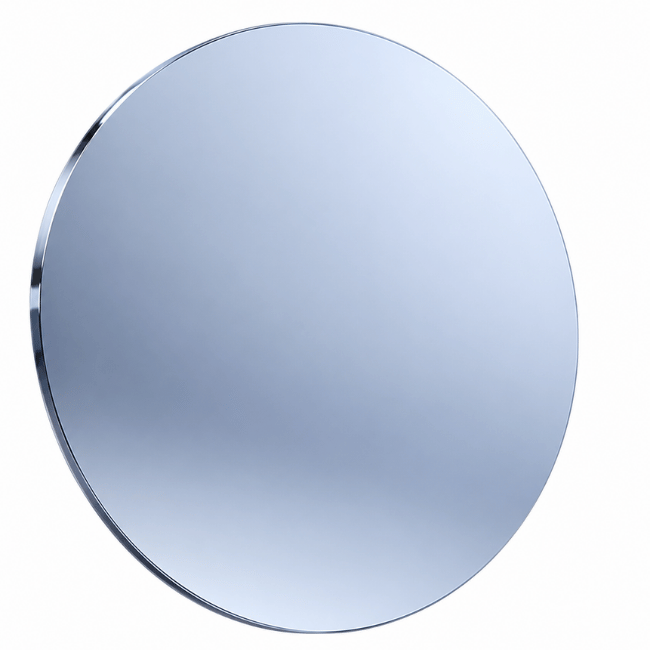
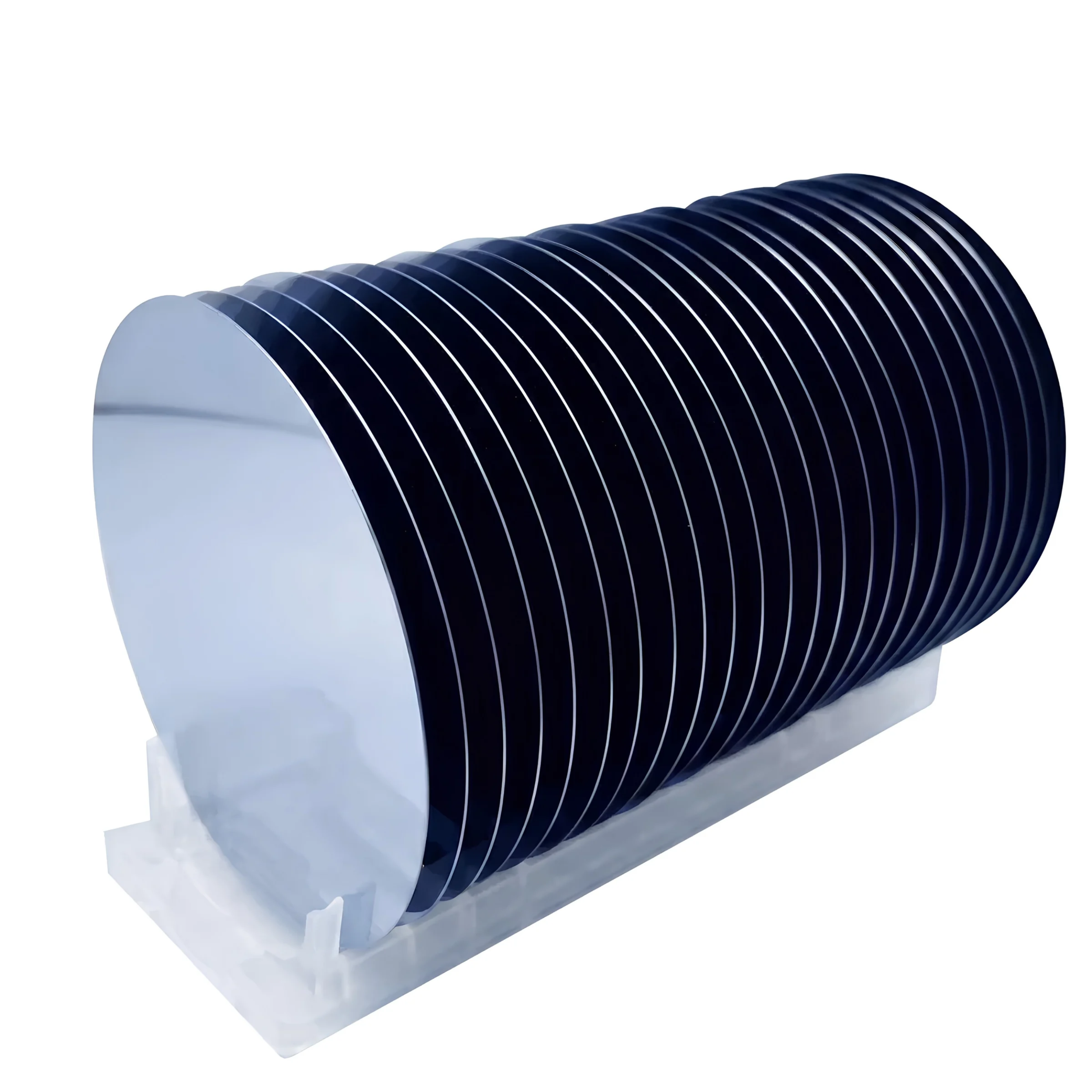
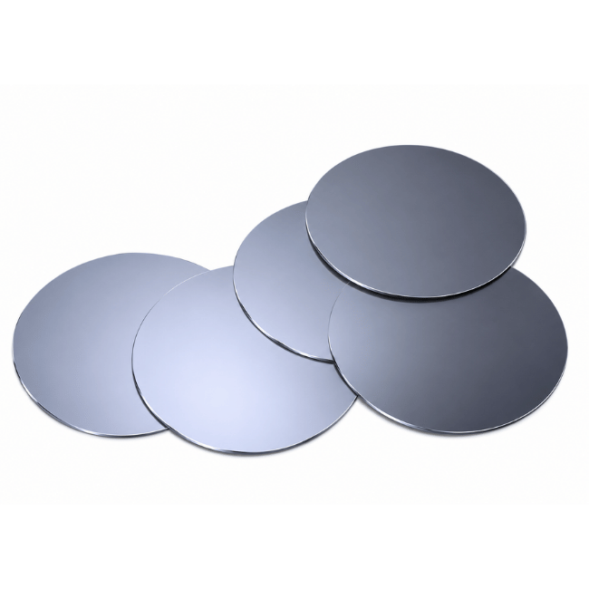
In 75 mm (3-inch) semiconductor manufacturing—often utilized for specialized compound semiconductors, RF devices, and legacy nodes—maintaining precise defect inspection is critical for yield. The 75 mm Calibration Wafer Standard supplies highly stable, NIST-traceable reference baselines that allow engineers to map the optical scattered signal intensity to actual physical particle dimensions. Compatible with KLA-Tencor Surfscan and equivalent platforms, these standards are vital for documenting tool qualifications (Qual-Dep™), monitoring drift, and optimizing wafer cleaning processes.
Deposition Variations:
-
Full Deposit: Complete surface coverage used for total tool qualification, verifying optical scan uniformity and detector response across the entire 75 mm surface.
-
1-Spot Deposit: A single targeted zone featuring one particle size, ideal for rapid baseline checks, routine drift monitoring, and single-threshold calibration.