
Last Updated: September 12, 2026
A single particle measuring 3nm can kill a transistor gate at the 3nm node (nist.gov). That is not a hypothetical. It is the daily reality of wafer fabrication, and it explains why semiconductor metrology tools have become the most scrutinized equipment in the fab. At Applied Physics, we have supplied calibration wafer standards and particle metrology systems to semiconductor and cleanroom operations since 1992, and the shift toward sub-5nm particle detection has reshaped what fabs demand from their inspection stack.
The challenge is straightforward to state and brutal to solve. As critical dimension shrinks, the size of a yield-killing defect shrinks with it. A particle that was cosmetic at the 28nm node becomes fatal at the 5nm node. That means defect review must resolve features and particles far below the wavelength of visible light, and it must do so across an entire 300 mm wafer without collapsing cycle time.
Below, we break down which semiconductor metrology tools actually deliver sub-5nm particle detection, where each technique hits its ceiling, and how to select an inspection stack that balances sensitivity against throughput and cost of ownership.
Semiconductor defect inspection techniques fall into two broad categories: optical methods that scan quickly across large areas, and electron or probe-based methods that resolve individual nanoscale defects at much slower rates. The practical question is never “which technique is best” but “which technique catches the defects that matter at the step I am inspecting.”
Most fabs run a hybrid stack. Optical inspection handles high-volume wafer screening. Electron-beam and atomic force methods handle defect review and critical dimension verification. The table below summarizes how the major techniques compare for sub-5nm work.
| Technique | Best Resolution | Throughput | Best For |
|---|---|---|---|
| Optical / laser scattering | ~10-20nm | Very high | High-volume surface contamination screening |
| SEM defect review | Sub-nm | Moderate | Defect classification and root-cause analysis |
| E-beam inspection | Sub-nm | Low | Critical layer defect capture |
| AFM | Atomic scale | Very low | Surface topography and CD verification |
Optical inspection hits a hard physical wall below 5nm. Diffraction limits the smallest feature a conventional optical system can resolve, and nanoscale defects scatter too little light to register above the noise floor (nist.gov). Fabs push optical tools with shorter wavelengths and advanced interferometry, but sensitivity to particles below 5nm remains marginal.
The workaround is statistical. Optical tools flag “hot spots” and process variation signatures rather than individual killer particles. That is useful for process control, but it cannot confirm whether a specific 3nm particle sits on a critical gate. For that confirmation, you need electron microscopy.
Laser scattering and SEM review serve opposite ends of the same workflow. Laser scattering inspection detects particles by measuring how they deflect a laser beam, which makes it fast and non-contact but size-limited by signal-to-noise ratio. SEM review images individual defects at sub-nanometer resolution, which makes it definitive but slow.
A common approach is to let laser scattering flag candidate defects, then route those coordinates to SEM review for classification. This two-stage flow keeps throughput high while preserving the sensitivity needed for sub-5nm particle detection.
Pro Tip The coordinates matter as much as the detection. If your laser scattering tool reports a defect position with poor accuracy, the SEM review step wastes hours hunting for a particle that has already moved or was never there. High-precision position coordinates are the hidden requirement in any hybrid inspection flow.
E-beam wafer inspection systems deliver the highest sensitivity available for sub-5nm defect capture, but that sensitivity comes at a throughput cost that reshapes how fabs schedule inspection. An e-beam tool raster-scans a focused electron beam across the wafer and collects secondary or backscattered electrons to form an image. Because the beam can be focused to a spot far smaller than any optical wavelength, the tool resolves defects that optical systems physically cannot see, including buried electrical defects that produce no topographical signature at all.
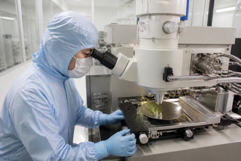
A process engineer in a cleanroom suit examining a semiconductor wafer under an electron-beam inspection system, with monitors displaying high-resolution wafer surface images in the background
The trade-off is speed, and it is not a small one. E-beam inspection is orders of magnitude slower per unit area than optical scanning because the beam must dwell at each pixel long enough to accumulate a usable signal-to-noise ratio. The practical levers an engineer controls are:
Multi-beam architectures are the main structural answer to the throughput wall. Instead of one beam, a multi-beam inspection tool splits the source into many parallel beamlets that image many regions of the wafer simultaneously. This preserves single-beam-class resolution while multiplying effective throughput, which is why multi-beam e-beam inspection has become the focus of advanced-node defect capture. The trade-off shifts from raw speed to complexity: beamlet uniformity, detector bandwidth, and data volume all become engineering constraints.
Fabs manage the remaining throughput gap by inspecting critical layers only, and by using e-beam for defect review rather than full-wafer screening. The decision of where to deploy e-beam inspection is one of the highest-value choices in the metrology budget, a full-wafer e-beam screen at production volume is rarely economic, but a targeted e-beam inspection on the layers where killer defects concentrate often pays for itself in caught escapes.
Watch Out Running e-beam inspection across a full 300 mm wafer at production volume will bottleneck your line. Restrict e-beam to critical layers and known defect-prone zones, or accept that inspection becomes the constraint on your cycle time.
The unique capability of e-beam inspection is voltage-contrast defect detection. A particle sitting on a gate is a physical defect that SEM review can image. But a partially open contact or a high-resistance via is an electrical defect that produces no topographical change, optical and AFM tools cannot see it, and even a standard SEM image looks normal. Voltage-contrast e-beam inspection biases the wafer so that defective electrical nodes charge differently from good ones, making the defect visible as a brightness contrast. For sub-5nm nodes, where a single marginal via can kill a device, this is often the only technique that catches the defect before it escapes to final test.
Atomic force microscopy measures surface topography by tracing a sharp probe across the wafer, achieving atomic-scale resolution that no optical or electron method matches for surface features. For critical dimension metrology, AFM verifies the actual physical width of sub-5nm features and confirms pattern fidelity after lithography.
The drawback is speed and probe wear. AFM is a point-by-point technique, so it samples small areas rather than scanning whole wafers. That makes it a verification tool, not a screening tool. Where AFM earns its place is in calibrating the other tools in the stack.
Every metrology tool is only as accurate as the standard it is calibrated against. Calibration wafer standards provide known, traceable reference features that let you verify whether your inspection system is actually detecting particles at the size it claims. Without a reliable standard, sub-5nm detection claims are unverifiable.
Applied Physics supplies calibration wafer standards across the common wafer sizes, including calibration wafer standards in 300 mm and smaller formats for legacy and R&D lines. These standards anchor the accuracy of both optical and electron-based semiconductor metrology tools.
Key Takeaway A metrology tool that drifts out of calibration will silently miss defects. Regular verification against a traceable calibration wafer standard is the cheapest insurance against a yield excursion you did not see coming.
Wafer contamination control standards define the particle thresholds a fab must hold, and the environmental requirements that make those thresholds achievable. Cleanroom classification, airflow, and filtration all set the baseline particle load that your inspection tools then have to measure against.
The ISO 14644 cleanroom classification standards establish the airborne particle limits that govern cleanroom operation, and semiconductor fabs typically run well below the general cleanroom classes. Environmental control is not a separate concern from metrology. If your cleanroom particle load is unstable, your inspection data will be noisy and your process control will chase phantom defects.
Cost of ownership for sub-5nm metrology is not the purchase price. It is the sum of capital cost, consumables, calibration, downtime, and the yield impact of defects the tool misses. Most cost-of-ownership discussions stop at the first four and ignore the fifth, which is the one that actually decides whether a tool pays for itself.
A workable framework breaks cost of ownership into four buckets:
1. Capital and depreciation. The tool’s purchase price amortized over its useful life, plus installation, facilities hookup, and any required cleanroom footprint. E-beam and multi-beam inspection tools carry the highest capital cost in the stack; optical inspection carries the lowest.
2. Recurring operating cost. Consumables (electron source emitters, AFM probes, optical lamps and detectors), calibration wafer standards, preventive maintenance, and the labor to run and maintain the tool. AFM probe wear is a real recurring line item, probes are consumables, not permanent fixtures.
3. Throughput cost. This is the bucket most models underweight. Every hour a wafer spends in inspection is an hour it is not producing revenue. A tool that is twice as sensitive but four times slower may cost more in cycle-time impact than it saves in caught defects. The right metric is cost per wafer inspected at a given sensitivity, not cost per tool.
4. Defect escape cost. The expected cost of defects the tool fails to catch, expressed as escape rate multiplied by the cost of a scrapped or degraded wafer at that process step. This is where the model gets hard, because escape rate is rarely known precisely. A common pattern is to bound it: estimate the cost of a single undetected killer particle at a critical layer, then ask how many escapes per thousand wafers the tool would have to prevent to justify its cost.
The decision rule that falls out of this framework is not ‘buy the most sensitive tool.’ It is: match tool sensitivity to the defect size that actually kills devices at that step, and match tool throughput to the cycle-time budget that step can tolerate. Over-inspecting a non-critical layer with an e-beam tool wastes capital and cycle time. Under-inspecting a critical layer with an optical tool lets killer particles escape.
Key Takeaway Build your cost-of-ownership model around defect escape rate and cycle-time impact, not sticker price. A cheaper tool that misses 3nm particles at a critical layer costs far more than a higher-priced tool that catches them, but a high-end tool deployed on a non-critical layer is just as wasteful.
One recurring cost that most cost-of-ownership models omit entirely is calibration and verification. Every metrology tool drifts. An e-beam tool’s beam current and detector gain drift with emitter age. An optical tool’s laser power and detector response drift with temperature and component aging. An AFM’s probe geometry changes as it wears. Without regular verification against a traceable calibration wafer standard, a tool can silently lose sensitivity to the exact particle sizes it was purchased to detect.
The cost of that verification is small, a calibration wafer standard and the labor to run a periodic check. The cost of skipping it is a yield excursion you did not see coming, discovered only when final test yields drop and the root cause traces back to a metrology tool that had been reporting ‘clean’ for weeks. In cost-of-ownership terms, calibration is the cheapest insurance in the model.
Metrology data feeds directly into computational lithography and process control, closing the loop between what you measure and what you print. Inspection results tell the lithography model where pattern fidelity is drifting, and process control uses that feedback to adjust the next run.
The integration opportunity most fabs miss is feeding metrology data back fast enough to matter. Inspection results that arrive a week after the lot has shipped cannot correct anything. Inline metrology that reports within the process window is what turns inspection from a post-mortem into a control input.
Sub-5nm particle detection is a stack problem, not a single-tool problem. Optical inspection screens, e-beam and SEM review classify, AFM verifies, and calibration wafer standards keep the whole chain honest. Get the balance wrong and you either miss killer defects or strangle your throughput.
Applied Physics has supported semiconductor metrology and contamination control since 1992, supplying calibration wafer standards across every common wafer size, nanoparticle size analyzers, and cleanroom monitoring systems built for rigorous process control. If your fab is moving to the 5nm node and needs sub-5nm detection you can actually verify, contact us to discuss calibration standards and metrology systems matched to your process.
Semiconductor metrology tools include scanning electron microscopy (SEM) for defect review, atomic force microscopy (AFM) for surface topography, transmission electron microscopy (TEM) for atomic-scale imaging, and optical inspection systems for high-throughput screening. For sub-5nm particle detection, E-beam inspection and laser scattering techniques are most effective. Calibration wafer standards ensure these tools maintain accuracy across wafer fabrication processes.
At the 3nm and 5nm nodes, a single particle larger than 5nm can bridge a transistor gate or short an interconnect, killing the die. As feature sizes shrink, the killer defect size shrinks with them. Yield enhancement depends on catching these nanoscale defects before they multiply across a wafer lot. Without sub-5nm detection capability, process control becomes reactive rather than predictive.
E-beam wafer inspection systems offer superior spatial resolution, resolving defects below 5nm that optical inspection cannot detect due to diffraction limits. However, E-beam throughput is significantly lower, making it suitable for defect review and targeted inspection rather than full-wafer screening. Optical systems remain faster for high-volume screening but miss nanoscale particles. A hybrid approach combines both for optimal sensitivity and speed.
Wafer contamination control standards include ISO 14644 for cleanroom classification, which specifies allowable particle concentrations per cubic meter. For semiconductor-specific requirements, SEMI standards govern surface contamination and particle measurement. Facilities must also comply with internal process control specifications.
The move to sub-5nm nodes raises the stakes on every measurement you make. Applied Physics provides calibration wafer standards in 300 mm, 200 mm, 150 mm, 125 mm, 100 mm, and 75 mm formats, plus nanoparticle size analyzers and cleanroom monitoring systems designed for semiconductor and cleanroom environments. Get started with Applied Physics and build a metrology stack you can trust at the node.
APPLIED PHYSICS TECHNICAL RESOURCE
Wafer inspection, SSIS calibration, particle deposition references, process control and semiconductor measurement workflows. Product and standards references should be interpreted for the actual instrument, facility, protocol and configuration.

Enter your details below to save your shopping cart for later. And, who knows, maybe we will even send you a sweet discount code :)
Allow notifications to get real-time updates about your shopping cart and who knows, you may even receive a sweet discount code 😊