
Last Updated: August 31, 2026
Sub-5nm defect detection is the process of identifying and measuring physical defects, such as particles, surface irregularities, and dimensional variations, at nanometer scales smaller than 5 nanometers in semiconductor wafers and components. This capability is critical for advanced semiconductor manufacturing, where defects at this scale can render entire chips unusable or cause performance degradation that violates yield requirements.
The term “sub-5nm” refers to the resolution threshold of the detection equipment. At this scale, traditional optical inspection methods reach their physical limits due to diffraction constraints. Specialized instrumentation, including atomic force microscopy, scanning electron microscopy, and condensation particle counters, must be deployed to achieve the precision necessary for modern fabrication nodes.
Defects at sub-5nm scales fall into several categories: particle contamination from the cleanroom environment, crystal defects introduced during processing, resist residue from lithography, and dimensional drift in features. Each type requires different detection strategies and measurement approaches. The challenge isn’t just finding these defects, it’s doing so reliably, repeatably, and without damaging the wafer or introducing new contamination during the inspection process itself.
Pro Tip The most overlooked aspect of sub-5nm defect detection is that your equipment is only as good as your calibration standards. A particle counter that hasn’t been calibrated against traceable wafer standards will give you false confidence in your data, and false confidence is worse than no data at all.
Semiconductor manufacturers operating at advanced nodes, 5nm, 3nm, and below, face yield challenges that didn’t exist at larger geometries. A single defect that would be invisible or inconsequential at 28nm can kill functionality at 3nm because the defect size approaches or exceeds the feature size itself.
The economic impact is direct. A wafer that costs between $10,000 and $15,000 to process becomes scrap if critical defects slip through undetected (semi.org). Multiply that across thousands of wafers per month, and the cost of missed defects becomes staggering. More importantly, defects that escape into customer products trigger recalls, warranty claims, and reputational damage that can cost millions.
Key Takeaway The real cost of defect detection isn’t the equipment investment, it’s the cost of defects you don’t catch. Every undetected defect that reaches a customer is exponentially more expensive than catching it in the fab.
Regulatory compliance and customer qualification also depend on strong defect detection. Customers purchasing advanced semiconductor components often require documented evidence that defect detection processes meet specific thresholds. Without sub-5nm detection capability, you cannot credibly claim compliance with those requirements.
Beyond yield and compliance, sub-5nm defect detection drives process improvement. By identifying where defects originate, whether in lithography, etch, deposition, or the cleanroom environment itself, manufacturers can implement targeted corrective actions. This feedback loop is essential for maintaining process stability as nodes shrink and defect budgets tighten.
Semiconductor metrology operates within established standards that define acceptable measurement uncertainty, calibration frequency, and traceability requirements. These standards ensure that defect detection results are comparable across facilities and defensible in customer audits.
According to SEMI International Standards for semiconductor manufacturing, metrology equipment used in advanced fabs must demonstrate measurement uncertainty below a specified threshold, typically 10-15% of the feature size being measured. At 5nm nodes, this means absolute measurement uncertainty must be in the sub-nanometer range, which is extraordinarily demanding.
Calibration standards themselves require traceability to national or international reference materials. For particle metrology, this means your particle counter must be validated against certified calibration aerosols traceable to NIST standards. For dimensional metrology, wafer calibration standards must be traceable to certified reference wafers with known feature dimensions.
The challenge is that calibration standards at sub-5nm scales are themselves difficult to produce and validate. Applied Physics provides calibration wafer standards specifically designed for advanced node metrology, offering traceable reference points that allow your equipment to be validated without guesswork.
Documentation and record-keeping are non-negotiable. Every calibration event, every equipment validation, and every defect detection result must be logged with timestamps, operator identification, and equipment serial numbers. This audit trail is what separates credible defect data from anecdotal observations.
Atomic Force Microscopy (AFM) and Scanning Electron Microscopy (SEM) represent the gold standard for sub-5nm defect characterization. AFM uses a mechanical probe scanning across the wafer surface to measure topography with sub-nanometer vertical resolution. SEM uses a focused electron beam to image surface features with nanometer-scale spatial resolution.
AFM excels at measuring surface roughness, step heights, and subtle topographic variations. The technique is non-destructive and doesn’t require sample preparation or conductive coatings. Applied Physics offers Atomic Force Microscopy systems with integrated scanning-probe and sample-stage designs that enhance anti-interference capability and simplify probe positioning. The precision laser and probe positioning device makes probe changing and spot adjusting straightforward, reducing setup time and operator error.
SEM, by contrast, provides superior lateral resolution and can detect both topographic and compositional defects through secondary electron imaging and energy-dispersive X-ray spectroscopy. SEM is faster than AFM for large-area surveys but requires more sample preparation and offers less quantitative vertical measurement capability.
The practical choice between AFM and SEM often depends on the defect type. Use AFM when you need precise height measurements or when the defect is subtle. Use SEM when you need rapid large-area screening or when you need to identify elemental composition.
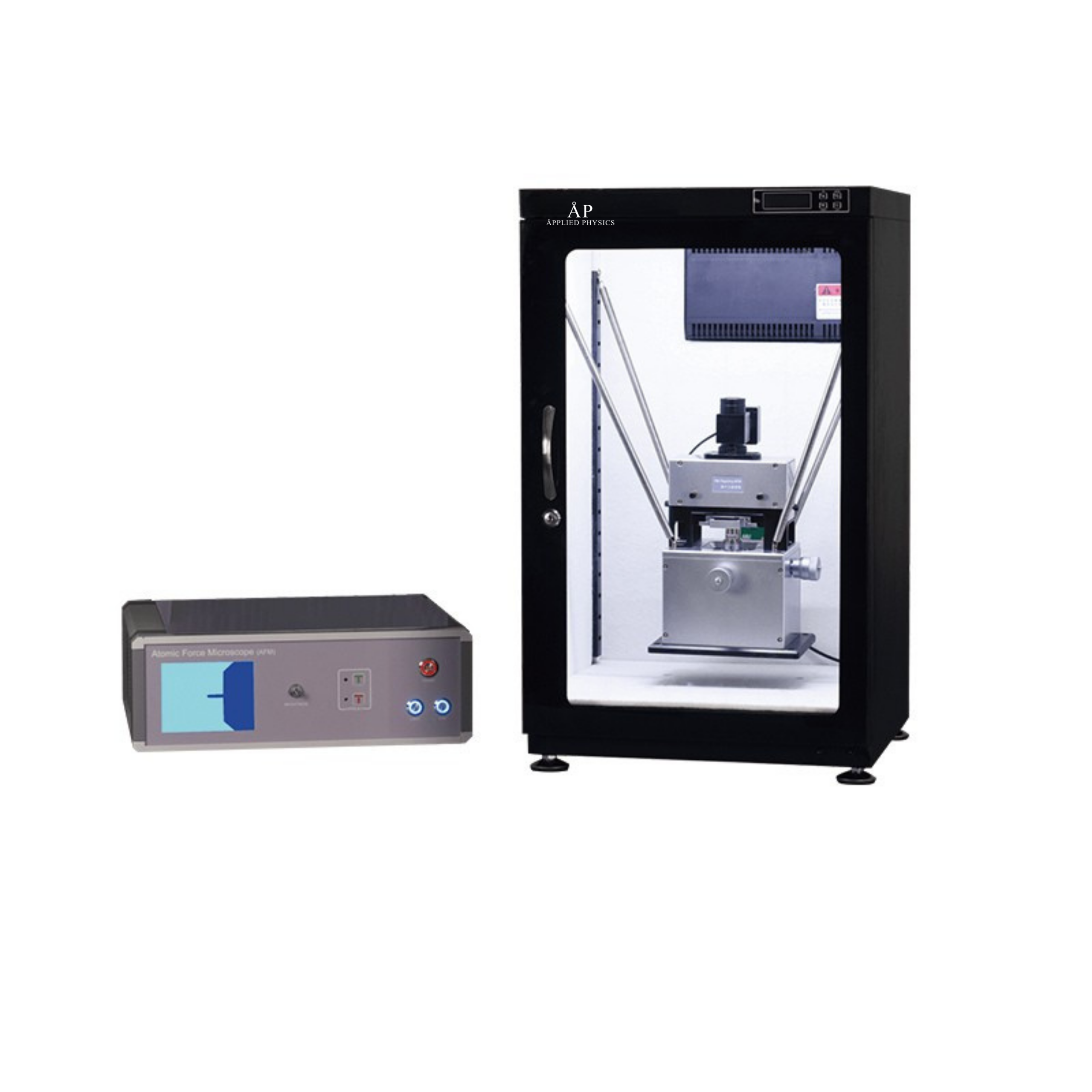
Close-up of precision atomic force microscopy equipment with scanning probe positioned above semiconductor wafer under controlled lighting in cleanroom environment
Watch Out A common mistake is running AFM or SEM without proper sample handling protocols. These instruments are sensitive to contamination and vibration. If your lab doesn’t have passive vibration isolation and active environmental control, your data will be noisy and unreliable.
Optical defect detection has fundamental physical limits at sub-5nm scales due to the wavelength of visible and near-infrared light. However, optical methods remain valuable for detecting larger defects, pattern anomalies, and surface contamination that might escape nanometer-scale techniques.
Particle detection, specifically, counting and sizing airborne particles in the cleanroom and on wafer surfaces, is a complementary approach. Particles larger than 0.1 micrometers can cause defects or yield loss at advanced nodes (peer-reviewed research). Condensation particle counters, like Applied Physics’s Handheld Condensation Particle Counter Model 3800, measure particle concentration in real time with sensitivity down to 0.01 micrometers.
These instruments work by drawing air through a chamber where particles are exposed to a supersaturated vapor. Particles act as nucleation sites, growing into droplets that can be counted optically. The result is a particle size distribution and total concentration, critical data for assessing cleanroom performance and predicting yield risk.
The relationship between airborne particle counts and wafer surface defects is well established but not deterministic. High particle counts increase risk, but some particles never land on the wafer, and some that do may not cause defects. Still, particle monitoring provides an early warning system and helps correlate environmental conditions with yield excursions.
Wafer calibration standards are reference wafers with precisely known feature dimensions, used to validate and calibrate metrology equipment. These standards are the foundation of traceability in semiconductor metrology.
A calibration wafer typically contains arrays of features at multiple sizes, lines, trenches, pillars, or other patterns, with dimensions verified by certified reference methods. When you measure these features with your AFM, SEM, or optical tool, you compare your measured values to the certified values. The difference is your measurement bias, which you then correct for in production measurements.
Applied Physics provides calibration wafer standards specifically engineered for sub-10nm applications. These wafers are manufactured with precision processing and characterized using traceable reference techniques, ensuring that your equipment validation is defensible in customer audits and regulatory inspections.
The practical challenge is that calibration standards degrade with use and exposure to the cleanroom environment. Particles land on the surface, oxidation occurs, and the certified dimensions may shift. This is why calibration standards require periodic re-certification and eventual replacement.
Pro Tip Schedule your wafer calibration standard re-certification annually, or more frequently if your tool is in heavy use. The cost of re-certification is trivial compared to the cost of making yield decisions based on drifted calibration.
Sub-5nm defect detection is only half the battle. The other half is preventing defects from occurring in the first place, which means controlling the cleanroom environment with precision.
Particles, chemical vapors, and ionic contaminants are the primary contamination vectors. Particles settle on wafers and create defects during subsequent processing steps. Chemical vapors deposit residues that interfere with lithography or etch processes. Ionic contamination causes corrosion and electrical failures.
Cleanroom design, HVAC systems, and material selection all contribute to contamination control. But measurement and validation are what confirm that control is actually working. This is where airflow visualization and particle metrology become essential tools.
Applied Physics specializes in cleanroom foggers for airflow visualization, tools that inject tracer particles into the cleanroom and allow operators to observe airflow patterns under actual operating conditions. This visualization reveals dead zones, turbulence, and bypass routes that could allow contamination to reach critical areas.
Combining airflow visualization with particle counting creates a complete picture: you see where the air is moving, and you measure what particles are in that air. This combination allows targeted remediation, whether that’s repositioning diffusers, sealing leaks, or improving material handling practices.
Before purchasing equipment or implementing new processes, understand your current defect landscape. What defects are you seeing? Where do they appear on the wafer? How frequently do they occur? What’s the correlation with process parameters or environmental conditions?
This baseline is established through a combination of wafer inspection, yield analysis, and cross-correlation with process data. You may use existing equipment, even if it’s not optimized for sub-5nm, to characterize your current defect population. The goal is to identify which defect types are causing the most yield loss and which are the highest priority to detect.
Document your findings in a defect classification scheme. Categorize defects by type (particle, crystal, resist residue, dimensional), location (edge, center, specific layer), and estimated size. This classification drives your equipment selection and measurement strategy.
Equipment selection depends on your defect priorities. If particles are your primary concern, invest in particle metrology and cleanroom monitoring tools. If dimensional defects dominate, prioritize AFM or SEM with sub-nanometer resolution.
Once equipment is installed, calibration is non-negotiable. Use certified calibration standards to validate measurement accuracy. Run blind samples, wafers measured by your equipment and also by an external reference lab, to verify that your results are traceable and defensible.
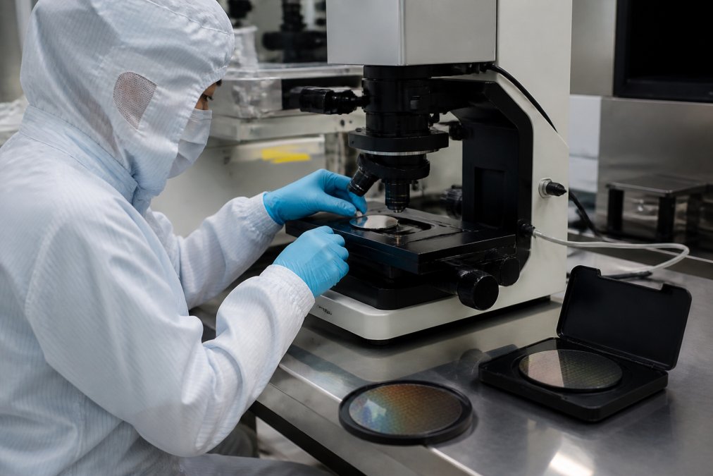
Process engineer or technician calibrating semiconductor metrology equipment at workstation with wafer samples and precision instrumentation under controlled lighting
Establish a calibration schedule. Most equipment requires monthly or quarterly validation; some require more frequent checks if used continuously. Document every calibration event, including the standard used, the date, the operator, and the results. This record is your evidence of due diligence.
Sub-5nm defect detection equipment is sophisticated and sensitive to operator technique. A poorly trained operator can generate unreliable data or damage the equipment. Invest in formal training for anyone who will use these tools.
Training should cover equipment operation, sample handling, calibration procedures, and data interpretation. Trainees should practice on known samples before running production wafers. Establish standard operating procedures that are documented, reviewed, and regularly updated.
Process validation means running a designed experiment to confirm that your defect detection method reliably identifies defects and produces repeatable results. This might involve seeded-defect wafers, wafers with intentional defects of known size and type, to verify that your equipment detects them consistently.
Document your validation results. This documentation becomes part of your quality system and provides evidence to customers and auditors that your defect detection process is fit for purpose.
The transition to sub-5nm defect detection surfaces several recurring challenges. Understanding these pitfalls helps you avoid them.
Equipment sensitivity to environmental conditions is one of the most underestimated problems. AFM and SEM require stable temperature, humidity, and vibration levels. A 1-degree Celsius temperature drift can shift measurement results by several nanometers. If your lab doesn’t have active environmental control, your data will scatter unpredictably. This isn’t a minor inconvenience, it’s a fundamental limitation that can invalidate your entire metrology program.
Calibration standard degradation creeps up gradually. You perform calibration, document the results, and assume your equipment is validated. Six months later, your calibration standard has drifted due to particle deposition or oxidation, but you don’t know it. Your equipment is now biased, and all your subsequent measurements are systematically wrong. Regular re-certification and proactive standard replacement prevent this trap.
Defect classification ambiguity arises when you’re trying to distinguish between different defect types at nanometer scales. Is that feature a crystal defect, a processing artifact, or measurement noise? Ambiguity leads to disagreement about which defects matter and which are acceptable. Establish clear classification criteria upfront and validate them against process impact data.
Operator variability in sample preparation and measurement technique can introduce scatter that masks real trends. This is why standardized procedures and regular training are essential. Some labs rotate operators through different instruments to cross-validate results and catch systematic biases.
The semiconductor industry continues to shrink feature sizes, pushing defect detection requirements toward even smaller scales. Sub-3nm nodes are already in early production, and sub-2nm is in development. This trend drives continued innovation in metrology technology.
Artificial intelligence and machine learning are beginning to play a role in defect detection. Rather than relying solely on threshold-based detection, AI models can be trained to recognize defect signatures in high-dimensional measurement data. This approach can improve defect capture rates and reduce false positives, though it introduces new challenges around model validation and explainability.
In-situ metrology, measurement performed during processing rather than after, is gaining traction. Real-time feedback allows process adjustments before defects propagate through multiple steps. This requires strong, fast measurement techniques that don’t damage the wafer or introduce contamination.
Cleanroom technology is also evolving. Advanced filtration, localized environmental control, and material innovations are reducing particle counts and chemical contamination to unprecedented levels. As cleanroom performance improves, the defect detection burden shifts from catching environmental contamination to detecting process-induced defects that are harder to prevent.
Applied Physics continues to invest in metrology innovation, developing next-generation calibration standards and particle detection tools that support the industry’s transition to even smaller nodes. The company’s 30+ years of experience in semiconductor and cleanroom applications position it to anticipate these trends and deliver solutions that keep pace with manufacturing demands.
Sub-5nm defect detection is no longer optional for advanced semiconductor manufacturers, it’s a competitive necessity. The equipment, standards, and processes required are sophisticated and demanding, but the alternative, undetected defects that reach customers, is far more costly. Applied Physics provides calibration wafer standards, particle metrology tools, and cleanroom visualization equipment specifically designed for advanced node production. Get started with Applied Physics and ensure your defect detection program is traceable, reliable, and audit-ready.
| Defect Detection Method | Best Application | Measurement Uncertainty | Speed |
|---|---|---|---|
| Atomic Force Microscopy | Topography, step height, subtle variations | Sub-nanometer | Slow (hours per wafer) |
| Scanning Electron Microscopy | Large-area survey, elemental composition | Nanometer-scale | Fast (minutes per wafer) |
| Optical Inspection | Pattern anomalies, large defects | 100+ nanometers | Very fast (seconds per wafer) |
| Particle Counting | Cleanroom monitoring, contamination assessment | 0.01 micrometer | Real-time continuous |
Sub-5nm defect detection directly impacts yield rates because defects at this scale propagate through multiple layers of semiconductor structures, causing device failures that may not appear until final testing. Detecting and eliminating these defects early prevents costly rework and scrap. As semiconductor nodes shrink below 5 nanometers, the margin for error shrinks proportionally, a single undetected defect can render an entire die unusable.
Atomic Force Microscopy (AFM) and Scanning Electron Microscopy (SEM) are the primary tools for sub-5nm defect detection, offering nanometer-scale resolution. Condensation Particle Counters detect airborne contamination that could introduce defects during fabrication. Optical inspection systems work alongside these tools for broader wafer assessment. The choice depends on your defect type: surface topology defects require AFM, while particle contamination requires particle counters and airflow visualization tools. Most advanced fabs use a layered approach combining multiple technologies.
Wafer calibration standards provide known reference structures at sub-5nm dimensions that allow your metrology equipment to verify measurement accuracy before scanning production wafers. These standards establish traceability and confirm your instruments are performing within specification. Without proper calibration standards, measurement drift goes undetected, leading to false passes or false failures. Calibration standards must be measured and certified to match your fab’s specific node requirements and process flows.
Cleanroom contamination control prevents particle defects from forming during wafer processing. Airflow visualization tools identify stagnant zones where particles accumulate, while particle counters measure contamination levels in real time. At sub-5nm nodes, even 0.1-micron particles can cause defects, making contamination control essential. Proper airflow patterns, gowning procedures, and equipment maintenance reduce defect introduction, directly supporting sub-5nm yield targets and GMP compliance.

Enter your details below to save your shopping cart for later. And, who knows, maybe we will even send you a sweet discount code :)
Allow notifications to get real-time updates about your shopping cart and who knows, you may even receive a sweet discount code 😊