
The high-precision world of Surface Mount Technology (SMT), the integrity of a solder joint is the difference between a high-performing device and a costly field failure.
Among various soldering defects, Cold Solder Joints remain one of the most elusive and detrimental.
Unlike a completely open joint, a cold solder joint might pass initial electrical testing while harboring structural weaknesses that lead to intermittent signals or total failure under thermal stress.
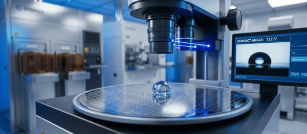
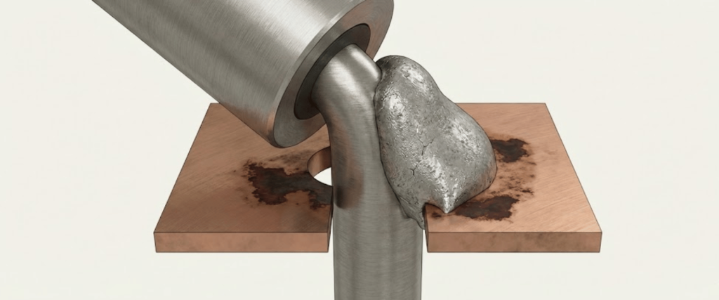
A cold solder joint occurs when the solder fails to melt completely or wet the PCB pad and component lead properly. This results in a grainy, dull, or lumpy appearance rather than the smooth, concave fillet expected in a quality joint.
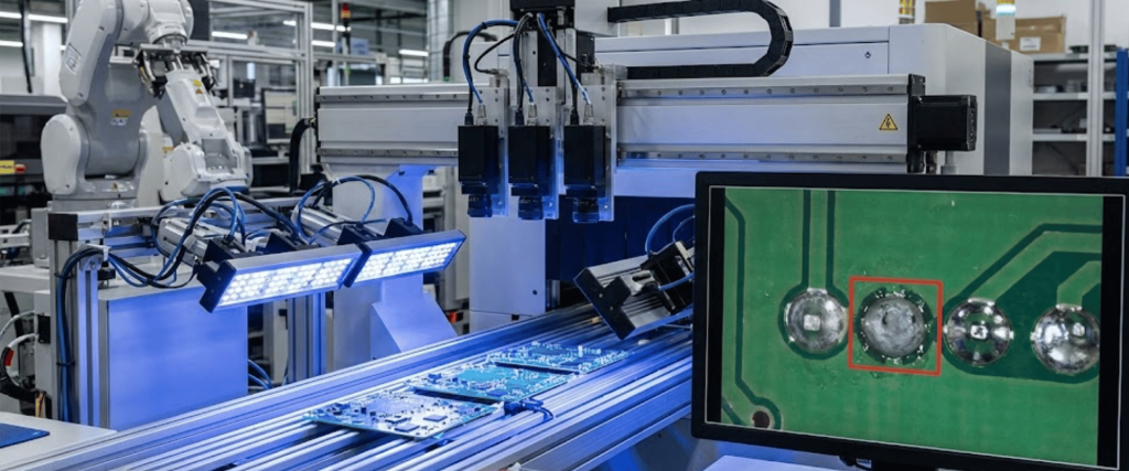
Detecting these defects requires more than just a glance. As components shrink to 01005 sizes, manufacturers must employ multi-layered diagnostic strategies.
AOI systems use high-speed cameras and complex algorithms to scan for visual irregularities. For cold joints, AOI looks for.
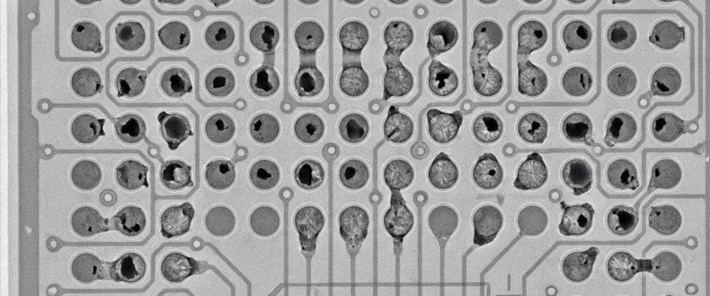
Visual inspection cannot see beneath BGA (Ball Grid Array) or QFN components. Advanced X-ray diagnostics allow technicians to see the internal structure.
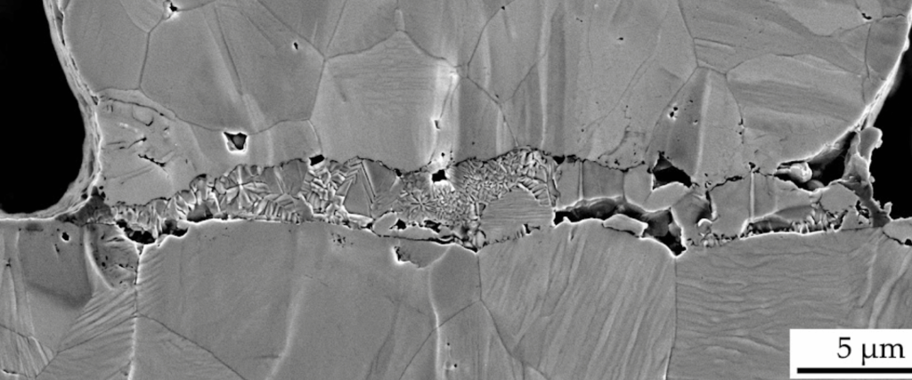
For failure analysis (FA), destructive testing is sometimes necessary.
| Method | Best For | Pros | Cons |
|---|---|---|---|
| AOI | Surface components | Fast, 100% coverage | Limited to line-of-sight |
| AXI (X-Ray) | BGA, QFN, hidden joints | Non-destructive, internal view | Higher equipment cost |
| SEM | Root cause analysis | Extreme detail | Destructive, time-consuming |
To maintain quality, diagnostic results must be measured against IPC-A-610 (Acceptability of Electronic Assemblies).
| Defect Type | Diagnostic Tool | IPC Class 3 Status |
|---|---|---|
| Cold Joint | 3D AOI / Visual | REJECT |
| Non-Wetting | X-Ray / SEM | REJECT |
| Disturbed Joint | 3D AOI | REJECT |
To eliminate cold solder joints, the focus must shift from detection to prevention.
Mastering advanced diagnostics for cold solder joints is essential for maintaining high-reliability electronics in the modern SMT landscape.
By integrating 3D AOI, X-ray inspection, and rigorous thermal profiling, manufacturers can detect hidden defects and ensure robust metallurgical bonds.
Adhering to IPC standards and implementing proactive prevention strategies significantly reduces field failures and costly rework.
Ultimately, a data-driven approach to soldering integrity guarantees superior product longevity and customer satisfaction.
A cold solder joint occurs when the solder never reaches its full melting point, resulting in poor wetting and a lack of chemical bonding. A disturbed joint, however, happens when the PCB or component moves while the solder is cooling down (the mushy stage), leading to a fractured internal crystalline structure. Both result in mechanical weakness, but their root causes, temperature vs. physical vibration, are different.
Standard 2D AOI is limited because it only captures a top-down view and may struggle to differentiate between a dull lead-free solder finish and a genuine cold joint. 3D AOI is much more reliable as it measures the volume, height, and angle of the solder fillet, allowing the system to identify the bulging or convex shapes typical of poor wetting associated with cold joints.
The Time Above Liquidus (TAL) is the duration for which the solder remains in a liquid state during reflow. If the TAL is too short, the solder doesn’t have enough time to chemically react with the copper pads to form a healthy Intermetallic Compound (IMC) layer. This results in a cold joint that may look connected but will fail under thermal or mechanical stress due to a lack of a metallurgical bond