
Table of Contents
- Why Semiconductor Yield Optimization Is Critical
- The Financial Impact of Yield Loss
- Traditional Inspection Methods vs. AI-Driven Approaches
- How AI Improves Defect Detection Accuracy
- Semiconductor Metrology Standards and Calibration
- Wafer Contamination Control and Defect Prevention
- Semiconductor Defect Reduction Strategies That Work
- Predictive Maintenance and Process Parameter Analysis
- Regulatory Compliance and Cost-Benefit Analysis
- Conclusion
- Frequently Asked Questions
Last Updated: September 4, 2026
Why Semiconductor Yield Optimization Is Critical
Semiconductor yield optimization maximizes functional integrated circuits from each silicon wafer by combining process engineering, metrology, and data science. It determines whether a fab operates profitably. At Applied Physics, we have spent decades supporting the metrology and contamination control side of this equation, and the stakes have never been higher as process nodes shrink toward their physical limits.
A modern fab costs billions to build, and every wafer carries fixed processing costs. When defect density rises, fewer usable chips emerge and that fixed cost spreads across smaller output. The difference between 75 percent and 90 percent yield on an advanced node can represent hundreds of millions in annual revenue.
The Financial Impact of Yield Loss
Yield loss translates directly into lost revenue. Every wafer processed represents material, equipment time, labor, and cleanroom overhead already spent. When yield drops, sunk costs remain constant while sellable output shrinks.
A 300 mm wafer contains far more die than a 200 mm wafer, so a single defect cluster can destroy hundreds of high-value devices. Advanced node wafers also carry higher per-wafer processing costs due to the number of deposition, etch, and lithography steps required.
Fab managers track two cost categories: direct cost of scrapped wafers and opportunity cost of lost production capacity. Reworking a process or running test wafers consumes cleanroom capacity that could otherwise produce sellable inventory.
Yield loss does not just reduce output; it inflates the effective cost per die and erodes the return on the billions invested in fabrication infrastructure.
Traditional Inspection Methods vs. AI-Driven Approaches
Traditional wafer inspection relies on rule-based optical systems and manual operator review. These systems scan for light scattering anomalies and flag potential defects for engineer classification. This approach has served the industry for decades but struggles with advanced node complexity.
As pattern layers become denser, nuisance defects far exceed true yield-killing defects. Operators spend hours reviewing false positives while genuine process excursions go unnoticed. Traditional systems cannot resolve the tradeoff between sensitivity and throughput.
AI-driven approaches shift classification from human eyes to machine learning algorithms. A deep learning model trained on historical defect data distinguishes between nuisance events and real pattern failures with greater consistency than manual review. Automated defect classification (ADC) assigns each anomaly to a category, allowing engineers to focus on yield-threatening events.
| Inspection Aspect | Traditional Rule-Based | AI-Driven Approach |
|---|---|---|
| Defect classification | Manual operator review | Automated defect classification |
| Nuisance defect handling | High false positive rate | False positive reduction via training |
| Pattern learning | Static rules | Continuous model refinement |
| Throughput | Limited by human review | High-speed inference at inspection tool |
| Adaptability | Requires recipe rewrite | Retrain on new data |
How AI Improves Defect Detection Accuracy
AI learns statistical patterns that distinguish real defects from process noise. A well-trained convolutional neural network identifies subtle anomalies in pattern layers and recognizes structural deviations from expected pattern geometry.
Training datasets are critical. A defect detection model is only as good as its labeled examples. Fabs build datasets by running wafers through inspection and having engineers classify thousands of defect images. A typical production-ready model requires 5,000 to 50,000 labeled defect images; models trained on fewer examples tend to overfit and fail with new defect morphologies (peer-reviewed research).
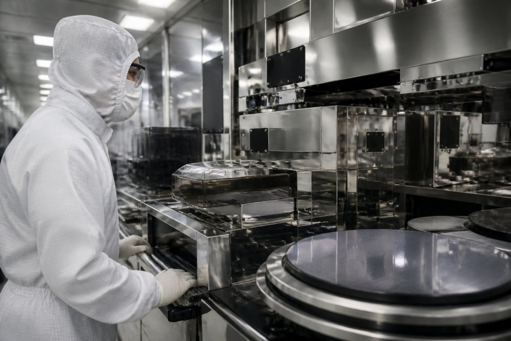
Model Deployment: Edge Processing vs. Cloud Analysis
Real-time inference at the inspection tool, edge processing, must complete within milliseconds to avoid slowing wafer throughput. A modern inspection tool scans a 300 mm wafer in 60 to 90 seconds (semi.org). This constraint typically limits edge models to smaller neural networks or specialized hardware accelerators (GPUs or FPGAs).
Centralized processing can run larger, more accurate models because latency is less critical. A fab sends inspection images to a central server where a complex model performs defect classification and correlates results across tools. This allows richer context but introduces delays of seconds to minutes. For real-time process control, that delay may be unacceptable; for offline root cause analysis, it is acceptable.
Most advanced fabs use a hybrid approach: a lightweight model runs on the inspection tool for immediate flagging, while a sophisticated model processes data centrally for detailed classification and trend analysis.
Human-in-the-Loop Validation and Continuous Improvement
Human-in-the-loop (HITL) workflows transition AI models from prototypes to production. After the model classifies an anomaly, an engineer reviews and confirms or corrects it. That correction feeds back into the training dataset for model retraining.
This feedback loop is essential because production defects are rarely static. New photomasks introduce new pattern geometries and process drift creates unfamiliar defect morphologies. Without continuous validation and retraining, model accuracy degrades as the fab’s process evolves.
HITL workflows operate at different review depths depending on confidence. High-confidence predictions (98%) are auto-sorted without review. Low-confidence predictions (60%) are flagged for immediate review. This tiered approach balances speed with accuracy.
HITL requires dedicated engineering time but delivers measurable benefits. Fabs report model accuracy improvements of 5 to 15 percentage points within six months as the model learns facility-specific defect signatures (peer-reviewed research).
When building a training dataset, include examples of normal process variation alongside confirmed defects. Models trained only on defect images tend to over-classify and flood engineers with nuisance alerts. A balanced dataset with roughly equal numbers of true defects and benign anomalies produces models with lower false positive rates in production.
Do not deploy a model to production without establishing a HITL review process. An unvalidated model may make confident predictions that are systematically wrong, leading engineers to trust incorrect classifications and miss genuine yield excursions.
Semiconductor Metrology Standards and Calibration
Semiconductor metrology standards are reference artifacts that ensure measurement tools produce accurate, repeatable results. Without calibrated standards, inspection tools drift over time, reporting particle sizes that are consistently larger or smaller than reality.
Calibration wafer standards are physical wafers with precisely known particle sizes and positions. Facilities use these to verify that particle counters and inspection systems detect events at the correct size threshold.
Calibration is not a one-time event. Tools drift as optics degrade and environmental conditions shift. Most facilities run calibration checks daily or weekly, tracking results to identify degradation before it affects production.
Skipping calibration to save a few hours of tool downtime is a false economy. An uncalibrated inspection tool can silently miss yield-killing defects for days before the error is discovered, contaminating process data and wasting far more production time than the calibration would have cost.
::: rapid glitch resolution.
Metrology standards support process control by providing a common reference across multiple tools. A shared calibration standard ensures measurements from different tools remain comparable.
Wafer Contamination Control and Defect Prevention
Wafer contamination control prevents particles, metallic impurities, and organic residues from reaching the wafer surface. Contamination is the leading cause of yield loss and becomes more damaging as feature sizes shrink.
Contamination sources include process tools, chemical baths, people, airborne particles, and wafer handling equipment. Each can deposit particles through contact or triboelectric charging.
Effective contamination control starts with the cleanroom environment. Airflow patterns must be validated to ensure particle-generating activities do not push contamination toward wafers. Cleanroom foggers generate visible vapor that follows air currents, confirming airflow moves contamination away from critical zones.
Wafer handling procedures matter. Automated systems reduce human contact but must be maintained to prevent particle generation. Chemical purity must be verified at point of use. Every material touching the wafer is a potential contamination source.
Semiconductor Defect Reduction Strategies That Work
Defect reduction strategies fall into three categories: prevention (stopping defects), detection (catching them early), and root cause elimination (removing underlying causes).
Prevention strategies focus on process stability through tight control of temperature, pressure, gas flow, and deposition time, plus rigorous material qualification.
Detection strategies rely on inspection infrastructure to find defects at the earliest possible process step. Early detection costs far less than discovering defects after dozens of additional processing steps.
Root cause elimination requires correlating defect data with process parameters, tool history, and environmental conditions. Modern fabs use predictive analytics to identify patterns that precede defect events, allowing intervention before production impact.
A practical defect reduction program follows a structured cycle: measure baseline defect density, identify dominant defect types, correlate with process parameters, implement corrective actions, verify improvement, and repeat.
Predictive Maintenance and Process Parameter Analysis
Predictive maintenance uses equipment sensor data to identify when a process tool is likely to fail or drift before it does. Sensor data contains early warning signals that precede equipment failure.
A deposition chamber with a degrading gas distribution plate produces wafers with increasingly non-uniform film thickness. Wafers may pass inspection but carry latent defects that emerge later. Hundreds of wafers may be processed before the marginal condition is detected.
Process parameter analysis examines relationships between process settings and yield outcomes. Machine learning identifies parameter combinations that correlate with high yield and flags conditions that precede yield loss.
Implementation involves collecting historical data linking process parameters to yield, training predictive models, and using them to guide process development and flag real-time deviations.
:::takeaway
The most valuable data in a fab is not the defect images themselves but the correlation between process conditions and yield outcomes. That correlation is what turns reactive defect fixing into proactive yield management.
Regulatory Compliance and Cost-Benefit Analysis
Semiconductor manufacturing operates under complex regulatory and customer-driven compliance requirements. Automotive customers require IATF 16949 compliance. Medical device manufacturers require ISO 13485 traceability. Military and aerospace applications demand MIL-PRF standards and detailed process documentation.
Equipment qualification and process validation require documented evidence of calibration, correlation studies, and process capability data. For AI systems, fabs must demonstrate that model classification accuracy meets or exceeds manual review accuracy, typically by running both in parallel on 1,000 to 5,000 defect images.
Building a Cost-Benefit Framework for Yield Improvement Investments
The cost-benefit analysis for yield improvement investments follows a straightforward framework, but the calculation requires understanding both the direct costs of the investment and the value of incremental yield.
Step 1: Establish baseline yield and defect density by measuring current yield and calculating defects per wafer or per 100 cm².
Step 2: Quantify the value of one percentage point of yield improvement. For a high-volume logic product with 60% gross margin and $100 per wafer ASP, a one percentage point improvement on 10,000 wafers per month generates $72,000 annual incremental profit. For specialty analog at $500 per wafer and 1,000 wafers per month, it generates $36,000 annually. Even fractional yield improvements generate substantial returns.
Step 3: Estimate yield improvement from the proposed investment using engineering judgment and historical data. AI-based defect classification typically delivers 2 to 5 percentage points over 12 months. Cleanroom airflow validation typically delivers 1 to 3 percentage points.
Step 4: Calculate total cost of ownership including capital equipment, implementation labor (500-2,000 hours), ongoing operational costs, and training. For AI defect classification, typical three-year TCO ranges from $500,000 to $2 million.
Step 5: Calculate payback period and ROI. A $1 million investment delivering 3 percentage points of yield improvement ($216,000 annually) has a 4.6-year payback. Five percentage points yields 2.8-year payback. Most fabs use a 2-3 year payback threshold.
Compliance as a Yield Enabler, Not Just a Cost
Compliance requirements often align with yield improvement. Rigorous process documentation for IATF 16949 builds data infrastructure for predictive analytics. Equipment qualification per SEMI standards validates reliable defect detection.
View compliance as integral to yield optimization, not a separate cost center. Compliance validation becomes part of the business case rather than overhead.
The most valuable data in a fab is not the defect images themselves but the correlation between process conditions and yield outcomes, combined with the financial impact of yield loss. That correlation, quantified in dollars, is what turns reactive defect fixing into proactive yield management and justifies investment in advanced inspection and process control systems.
| Investment Area | Typical Cost Driver | Expected Yield Benefit | Payback Period (Typical) |
|---|---|---|---|
| Metrology calibration standards | Recurring standard purchase ($50K-$150K/year) | 0.5-1.5 percentage points | 6-12 months |
| AI defect classification | Model development, training data, integration ($500K-$2M) | 2-5 percentage points | 2-4 years |
| Airflow visualization validation | Fogger and testing labor ($100K-$300K) | 1-3 percentage points | 1-2 years |
| Predictive maintenance software | Platform and sensor integration ($200K-$800K) | 1-2 percentage points | 2-3 years |
| Combined program (all four) | $850K-$3.25M | 4-11 percentage points | 1-2 years |
Conclusion
Semiconductor yield optimization directly determines the financial viability of advanced node manufacturing. As process geometries shrink and wafer costs rise, the margin for error narrows. Successful fabs combine rigorous metrology standards, proactive contamination control, and data-driven defect analysis.
At Applied Physics, we provide precision contamination control and semiconductor metrology solutions, including calibration wafer standards and cleanroom airflow visualization equipment, backed by decades of experience since 1992.
Get started with Applied Physics and put precision metrology and contamination control to work protecting your yield.
Frequently Asked Questions
What are the primary causes of yield loss in wafer fabrication?
Yield loss stems from multiple sources: contamination during fabrication, defects in pattern layers, process parameter drift, and design-related issues. Nuisance defects, minor imperfections that don’t affect circuit function, often mask yield-killing defects that render chips non-functional. Effective semiconductor yield optimization requires distinguishing between these categories and addressing root causes through contamination control, inspection recipe refinement, and real-time process monitoring.
How do metrology standards influence semiconductor yield?
Semiconductor metrology standards establish the precision baseline for detecting particles and defects. Calibration wafer standards enable accurate defect capture rates during wafer inspection, ensuring that anomaly detection systems catch actual problems rather than false positives. Proper calibration of particle counters and inspection equipment directly affects yield-killing defect identification, making standards compliance essential for high-volume semiconductor manufacturing.
Why is wafer contamination control essential for yield improvement?
Contamination introduces particles that create defects during the fabrication process. Wafer contamination control, through cleanroom monitoring, airflow management, and equipment validation, prevents these particles from reaching pattern layers. Even trace contamination can trigger yield loss at advanced nodes. Integrated systems that combine real-time monitoring with design-based inspection recipes catch contamination-induced defects early, reducing scrap and rework costs.
How does yield optimization impact semiconductor manufacturing costs?
Each percentage point of yield loss translates to direct material waste and reduced output per wafer start. At advanced nodes, the cost per defective die is substantial. Yield optimization through improved defect detection, contamination control, and predictive analytics reduces scrap, lowers cost-per-good-die, and improves throughput optimization. The investment in precision inspection equipment and monitoring systems pays back through reduced manufacturing waste and faster time-to-volume.
This content was published by Applied Physics, a provider of precision contamination control, semiconductor metrology, and specialized medical equipment for critical manufacturing environments.
