Last Updated: July 27, 2026
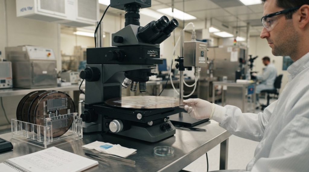
Semiconductor metrology equipment for sale represents one of the most critical investments in advanced manufacturing today. At Applied Physics, we understand that precision measurement systems drive yield improvement, process optimization, and competitive advantage across wafer fabrication facilities worldwide. Whether you’re sourcing new instruments or evaluating used equipment options, the choice between optical systems, electron beam metrology, and film-thickness analyzers directly impacts your production node capability and bottom-line profitability.
The semiconductor inspection equipment market continues to expand as manufacturers push toward smaller nodes, 3D architectures, and advanced packaging techniques. Metrology tools are no longer optional add-ons, they’re foundational to maintaining process control and meeting yield targets. This guide walks you through the landscape of available metrology equipment, the technical distinctions between major tool categories, pricing models for new versus used systems, and practical evaluation criteria to match equipment specifications to your production requirements.
Semiconductor metrology equipment encompasses a broad range of precision instruments designed to measure critical dimensions, film thickness, surface topology, and defect characteristics on wafers and semiconductor devices. These tools fall into several functional categories: critical dimension measurement systems (CD-SEM, optical CD), film-thickness analyzers, defect detection platforms, and surface characterization instruments.
The distinction matters because each tool serves a specific process control function. A CD-SEM measures feature widths and heights with nanometer precision. A film-thickness measurement system uses spectroscopic ellipsometry or ultrasonic techniques to characterize dielectric and metal layers. Defect detection systems scan wafer surfaces for particles, voids, and pattern anomalies. Applied Physics calibration wafer standards support these instruments by providing traceable reference materials that ensure measurement accuracy and repeatability across production runs.
Precision measurement is the foundation of semiconductor process control. Without accurate metrology, manufacturers cannot detect process drift, validate recipe changes, or identify yield-limiting defects. A single measurement error, whether in critical dimension or film thickness, can cascade through hundreds of wafers before detection, resulting in significant scrap and rework costs.
Modern semiconductor manufacturing operates at the edge of what physics allows. At advanced nodes, a 1-nanometer error in feature width can shift device performance characteristics or cause complete functional failure. This is why semiconductor metrology equipment for sale commands significant capital investment and why selection criteria must account for precision specifications, throughput requirements, and long-term calibration stability.
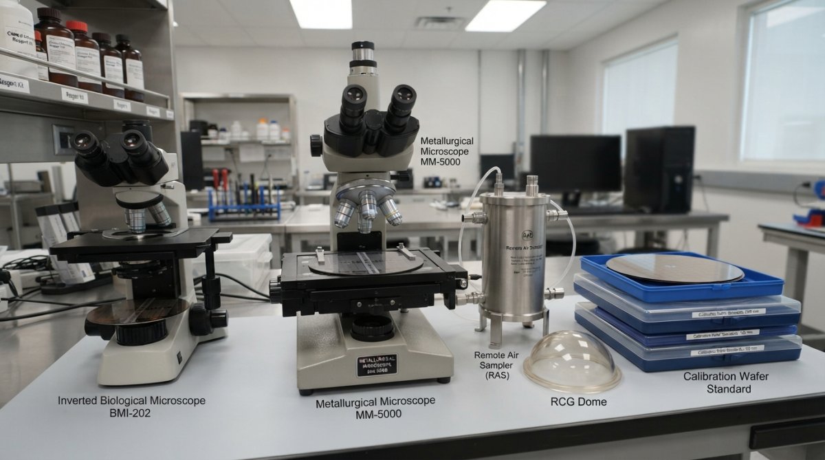
The metrology equipment landscape divides into several major technology categories, each optimized for different measurement challenges and production environments. Understanding these distinctions helps you match tool capabilities to your specific process control needs.
Optical metrology systems use light-based measurement principles to analyze wafer properties without damaging samples. Fourier-transform infrared (FT-IR) spectroscopy measures film composition and thickness by analyzing how samples absorb infrared radiation at specific wavelengths. These systems excel at characterizing transparent films, oxides, nitrides, and polymers, where optical techniques provide non-destructive, high-speed measurement.
Optical critical dimension (OCD) tools measure feature dimensions using reflected light and advanced algorithms to infer nanoscale structure from optical signatures. They offer advantages over electron beam systems in throughput and cost, though they’re limited to features above approximately 20 nanometers. For many manufacturing environments, optical systems provide the right balance of speed, accuracy, and operational simplicity. Applied Physics calibration wafer standards support optical metrology validation by providing traceable references with certified film thickness and optical properties across standard wafer sizes, 150 mm, 200 mm, and 300 mm formats.
Critical dimension scanning electron microscopy (CD-SEM) delivers the highest spatial resolution for feature measurement, reaching sub-nanometer precision on gate lengths, trench depths, and interconnect widths. Electron beam systems physically scan the wafer surface with a focused electron beam, collecting secondary electrons that form high-resolution images. Advanced systems like the Applied Materials VeritySEM 10 CD-SEM and Hitachi High-Tech GT2000 incorporate specialized detectors optimized for 3D device structures, gate-all-around transistors, 3D NAND, and complex interconnect architectures.
The tradeoff is operational complexity and cost. CD-SEM tools require trained operators, regular calibration, and careful sample preparation. Throughput is lower than optical systems, typically 10-30 measurements per hour versus hundreds per hour for optical tools. However, for advanced logic and memory manufacturers working at modern nodes, CD-SEM capability is non-negotiable.
Film-thickness measurement systems employ multiple technologies depending on the material and accuracy requirements. Spectroscopic ellipsometry measures optical properties to infer thickness of transparent films. Pulse ultrasonic methods measure metal film thickness non-destructively. X-ray fluorescence (XRF) quantifies elemental composition and thickness for thin films.
Defect detection systems scan entire wafer surfaces using optical or acoustic techniques to identify particles, voids, scratches, and pattern defects. These tools operate at high throughput, scanning a 300 mm wafer in minutes, making them essential for inline process monitoring. Rudolph Technologies MetaPulse series and similar platforms combine multiple measurement modalities to characterize wafer flatness, defects, and film properties in single-pass analysis.
The decision between new and used semiconductor metrology equipment for sale involves balancing capital investment, operational risk, maintenance requirements, and technology currency. Both paths are viable, but the evaluation criteria differ significantly, and the true cost of ownership extends far beyond the purchase price.
New metrology systems from major suppliers, Applied Materials, Bruker, Hitachi High-Tech, and others, typically cost between $500,000 and $3 million depending on capability. Entry-level optical CD systems start around $400,000. Advanced CD-SEM platforms exceed $2 million. Bruker’s Automated AFM systems for nanoscale surface characterization require direct contact for pricing but represent significant capital investment for specialized applications.
New equipment includes manufacturer warranty, ongoing software support, and access to the latest calibration standards. Vendors provide training, application support, and regular maintenance contracts. For manufacturers operating at modern nodes or requiring state-of-the-art measurement capability, new equipment is often the only viable option because used systems may lack the precision specifications or feature support needed for advanced processes.
The used metrology equipment market offers significant cost savings, typically 40-60% below new equipment pricing. A used CD-SEM might cost $800,000 to $1.2 million versus $2+ million for a new system. Used optical metrology systems range from $100,000 to $400,000 depending on age, condition, and remaining calibration certification.
Sourcing used equipment requires careful evaluation of equipment history, maintenance records, and remaining measurement accuracy. Many used systems come from fab consolidations, technology transitions, or equipment upgrades. Reputable resellers provide equipment refurbishment, recalibration, and limited warranties. However, purchasing used equipment without proper technical evaluation introduces risk, measurement drift, component wear, or obsolete software can compromise process control.
Applied Physics calibration wafer standards support validation of both new and used metrology equipment. Before deploying a used system into production, run measurement verification against certified calibration standards to confirm the equipment meets your process control specifications.
Total cost of ownership (TCO) includes equipment purchase, installation, training, spare parts, calibration, and maintenance over the system’s operational life (typically 7-10 years). For a $1 million CD-SEM system, the true TCO often reaches $1.8-$2.4 million over its lifetime, meaning the purchase price represents only 40-55% of total cost.
Annual maintenance and service costs typically run 8-12% of equipment purchase price. A $1 million CD-SEM system incurs $80,000-$120,000 in annual maintenance. However, this figure masks significant variation by equipment age and type:
For used equipment purchased in year 4 or later of its operational life, budget for elevated maintenance costs immediately. A used CD-SEM purchased with 5 years of operational history should assume 12-15% annual maintenance costs from day one, not the 8% figure that applies to new systems.
Calibration and preventive maintenance are non-negotiable cost drivers that many buyers underestimate.
Calibration frequency and cost:
Preventive maintenance schedules:
Most systems require quarterly or semi-annual service visits. Plan maintenance during production downtime to minimize impact on wafer processing schedules. Unplanned downtime due to deferred maintenance typically costs 3-5x more than scheduled preventive maintenance.
Spare parts inventory adds significantly to TCO and operational risk. Critical components like detector modules, electron optics, and optical systems may require 6-month lead times if not stocked. Maintaining $50,000-$150,000 in spare parts inventory is common for large fabs operating multiple metrology systems.
For used equipment, spare parts availability becomes a critical risk factor. Equipment manufactured 8+ years ago may have components that are no longer in production. Obsolete parts require either expensive custom fabrication or equipment replacement. Before purchasing used equipment, verify with the manufacturer or reseller that spare parts remain available and confirm typical lead times.
Purchasing used semiconductor metrology equipment for sale requires compliance verification that many buyers overlook until deployment.
FDA and regulated manufacturing environments:
If your facility operates under FDA oversight (pharmaceutical manufacturing, medical device production, or contract manufacturing for regulated industries), metrology equipment must meet specific regulatory requirements. FDA 21 CFR Part 11 governs electronic records and signatures. Equipment must demonstrate data integrity, audit trail capability, measurement traceability, and documented calibration history. Used equipment lacking documented calibration records or data validation capability may not meet regulatory requirements and could trigger FDA observations during inspections.
SEMI standards and safety compliance:
The Semiconductor Equipment and Materials International (SEMI) publishes safety and performance standards for semiconductor equipment. Used equipment imported into the United States must comply with SEMI standards for electrical safety, vacuum system integrity, and operational safety. Equipment manufactured before 2010 may not meet current SEMI standards without retrofitting.
Import/export and tariff considerations:
Used semiconductor equipment imported from overseas may be subject to tariffs, import duties, and customs compliance requirements. Equipment exported from the United States may require export licenses depending on destination country and equipment capability. Budget for customs clearance, tariff costs (typically 2-5% of equipment value), and potential delays of 4-8 weeks for international shipments.
Before purchasing used equipment, consult your quality assurance and regulatory affairs teams. Require the seller to provide:
Budget for independent validation testing to confirm the equipment meets your measurement specifications and regulatory requirements before production deployment. Validation testing typically costs $5,000-$15,000 and requires 2-4 weeks of lab time.
| Cost Category | New Equipment (Year 1) | Used Equipment (Year 1) | New Equipment (Year 5) | Used Equipment (Year 5) |
|---|---|---|---|---|
| Purchase Price | $1,000,000 | $400,000-$600,000 | N/A | N/A |
| Installation & Training | $50,000-$100,000 | $10,000-$30,000 | N/A | N/A |
| Annual Maintenance (8%) | $80,000 | $32,000-$48,000 | $80,000 | $48,000-$72,000 |
| Calibration (Monthly) | $36,000 | $36,000 | $36,000 | $36,000 |
| Spare Parts Reserve | $15,000 | $15,000 | $20,000 | $25,000 |
| Annual TCO | $181,000 | $93,000-$129,000 | $136,000 | $109,000-$133,000 |
| 5-Year Cumulative | $1,000,000 + $750,000 = $1,750,000 | $500,000-$700,000 + $450,000 = $950,000-$1,150,000 | , | , |
Semiconductor inspection equipment serves dual purposes: detecting defects that escape process control and validating that process recipes remain centered on target specifications. This dual role makes metrology equipment for sale one of the highest-value investments in a fab’s quality infrastructure.
Defect detection systems scan wafer surfaces at high speed to identify particles, voids, and pattern anomalies that indicate process problems. Modern systems combine optical and acoustic sensing to achieve sensitivity down to 0.1-micrometer particles on 300 mm wafers. Throughput matters, a defect detection system that scans a wafer in 3 minutes enables inline monitoring without slowing production. A system requiring 15 minutes per wafer becomes a bottleneck.
Throughput optimization involves matching tool capability to your production volume and process requirements. High-volume logic fabs require rapid scanning across entire wafer surfaces. Specialty fabs producing fewer wafers can accept longer scan times if measurement sensitivity is superior. The tradeoff is fundamental: faster scanning often requires accepting slightly lower defect sensitivity, while maximum sensitivity typically requires longer measurement times.
Semiconductor metrology equipment must meet strict reliability and accuracy standards. The Semiconductor Industry Association (SIA) and International Organization for Standardization (ISO) publish specifications for measurement uncertainty, repeatability, and reproducibility. Equipment must demonstrate measurement stability over weeks and months of operation without recalibration.
Reliability testing involves running the same wafer through the metrology system repeatedly and comparing results. Repeatability, the variation in successive measurements of the same location, must be better than 3-sigma of the specification window. Reproducibility, variation across different operators, different times, and different environmental conditions, must demonstrate the system provides consistent results under production conditions.
Applied Physics supports this validation process by providing calibration wafer standards with certified optical properties, film thickness values, and defect characteristics. These standards enable you to verify that your metrology equipment maintains measurement accuracy and detect drift before it impacts production decisions.
The metrology equipment market includes both large diversified suppliers and specialized vendors. Understanding the competitive landscape helps you evaluate equipment options and assess long-term vendor viability.
Applied Materials dominates the CD metrology market with the VeritySEM 10 platform, which combines sub-nanometer electron beam resolution with advanced detectors optimized for EUV and high-NA EUV lithography. The system captures 13-36 critical dimension measurements across the wafer in fast cycles, enabling rapid process feedback.
Bruker’s Automated AFM systems provide nanoscale surface characterization for inline process control and advanced packaging applications. The systems feature fully automated operation, high repeatability, and customizable service support. Bruker’s positioning emphasizes measurement reliability and application expertise across semiconductor, MEMS, and advanced packaging segments.
Hitachi High-Tech’s GT2000 platform targets high-precision electron beam metrology for 3D device structures. The system includes enhanced detection for back-scattered electrons, enabling imaging of complex device architectures like gate-all-around transistors and 3D NAND memory.
Rudolph Technologies (now part of Onto Innovation) supplies wafer testing and film-thickness metrology systems. The MetaPulse series offers non-destructive ultrasonic film-thickness measurement and integrated optical analysis for comprehensive wafer characterization.
Applied Physics has delivered precision contamination control and semiconductor metrology solutions since 1992. Our calibration wafer standards provide traceable reference materials essential for validating metrology equipment accuracy and maintaining measurement confidence across production runs.
We offer calibration wafer standards in three standard sizes, 150 mm, 200 mm, and 300 mm, with certified optical properties and film thickness values. These standards support optical metrology validation, FT-IR spectroscopy calibration, and CD-SEM measurement verification. By maintaining calibrated reference materials, you establish a measurement traceability chain that satisfies quality audits and supports continuous process improvement.
Applied Physics standards integrate into your metrology validation workflow without requiring specialized expertise. Use them to verify new equipment before deployment, monitor measurement drift in operating systems, and establish baseline accuracy for process control decisions.
Capital investment in metrology equipment requires careful financial planning. The direct equipment cost represents only one component of total cost of ownership.
Total cost of ownership (TCO) includes equipment purchase, installation, training, spare parts, calibration, and maintenance over the system’s operational life (typically 7-10 years). Annual maintenance costs typically run 8-12% of equipment purchase price. A $1 million CD-SEM system incurs $80,000-$120,000 in annual maintenance.
Calibration and preventive maintenance are non-negotiable. Metrology equipment drifts over time as components age and environmental factors accumulate. Monthly or quarterly calibration using certified reference standards prevents drift from impacting process decisions. Preventive maintenance, replacing wear components before failure, extends equipment life and maintains measurement reliability.
Spare parts inventory adds to TCO. Critical components like detector modules, electron optics, and optical systems may require 6-month lead times if not stocked. Maintaining $50,000-$150,000 in spare parts inventory is common for large fabs operating multiple metrology systems.
Training and operator expertise represent significant but often-overlooked TCO elements. CD-SEM operators require 2-4 weeks of intensive training. Optical system operators need 1-2 weeks of training. Retaining skilled operators reduces measurement errors and extends equipment life.
Purchasing used semiconductor metrology equipment for sale requires compliance verification. If the equipment was originally installed in a regulated environment (pharmaceutical manufacturing, medical device production), regulatory agencies may require documentation of equipment history and performance validation before deployment in your facility.
FDA 21 CFR Part 11 governs electronic records and signatures in regulated environments. If your facility operates under FDA oversight, metrology equipment must demonstrate data integrity, audit trail capability, and measurement traceability. Used equipment lacking documented calibration history or data validation capability may not meet regulatory requirements.
Before purchasing used equipment, consult your quality assurance and regulatory affairs teams. Require the seller to provide complete equipment history, maintenance records, and calibration documentation. Budget for independent validation testing to confirm the equipment meets your measurement specifications before production deployment.
Selecting the right metrology equipment requires matching tool specifications to your process requirements. This evaluation matrix helps structure the decision process and provides the technical depth most competitors skip.
The following matrix compares key technical specifications across major metrology equipment categories. Use this framework to evaluate whether specific tools meet your production requirements.
| Specification | Optical CD | CD-SEM | Spectroscopic Ellipsometry | Defect Detection (Optical) | AFM/Nanoscale |
|---|---|---|---|---|---|
| Measurement Resolution | 5-20 nm (feature-dependent) | 0.5-2 nm (sub-nanometer) | 0.1-1 nm (film thickness) | 0.1-0.5 µm (particle detection) | 0.1 nm (surface topology) |
| Measurement Uncertainty (3-sigma) | ±2-5% of feature size | ±1-3% of feature size | ±0.5-2 nm absolute | ±10-20% of particle size | ±0.5-1 nm absolute |
| Throughput (wafers/hour) | 15-30 | 2-6 | 10-20 | 1-3 | 0.5-2 |
| Measurement Time per Wafer | 2-4 minutes | 10-30 minutes | 3-6 minutes | 20-60 minutes | 30-120 minutes |
| Wafer Size Compatibility | 150 mm, 200 mm, 300 mm | 150 mm, 200 mm, 300 mm | 150 mm, 200 mm, 300 mm | 150 mm, 200 mm, 300 mm | 150 mm, 200 mm (300 mm rare) |
| Feature Size Range | 20 nm-10 µm | 5 nm-5 µm | Blanket films (all sizes) | 0.1 µm-100 µm | 1 nm-10 µm |
| Material Specificity | Patterned features only | Patterned features only | Dielectric & transparent films | All materials (particles) | All materials (surface) |
| Operator Skill Required | Low-Medium | High | Medium | Low-Medium | High |
| Maintenance Interval | Quarterly | Monthly-Quarterly | Quarterly | Semi-annual | Monthly |
| Typical Equipment Cost (New) | $400K-$800K | $1.5M-$2.5M | $250K-$600K | $600K-$1.2M | $1M-$2M |
| Typical Equipment Cost (Used) | $100K-$300K | $800K-$1.2M | $75K-$250K | $200K-$500K | Contact supplier |
Key interpretation notes:
Technology node determines measurement requirements:
28 nm and above (Mature nodes): Optical metrology systems meet most requirements. Feature sizes are large enough that optical diffraction limits (20 nm) don’t constrain measurement. Throughput is excellent, and operator skill requirements are low. Cost is moderate. Recommendation: Optical CD systems are sufficient; consider defect detection for yield monitoring.
14 nm to 7 nm (Advanced nodes): CD-SEM capability becomes necessary for critical dimension measurement of gate lengths, fin widths, and interconnect dimensions. Optical systems lose accuracy below 20 nm because diffraction effects dominate. Recommendation: Deploy CD-SEM for critical dimensions; use optical systems for non-critical features to preserve throughput.
5 nm and below (Cutting-edge nodes): Advanced CD-SEM systems with enhanced 3D imaging capability are required. Gate-all-around transistors, extreme ultraviolet (EUV) lithography, and 3D device structures demand sub-nanometer measurement precision. Standard CD-SEM systems may lack the detector sensitivity or image processing capability for these structures. Recommendation: Invest in latest-generation CD-SEM (Applied Materials VeritySEM 10 or Hitachi GT2000 equivalent); budget for specialized training and extended maintenance support.
Wafer size affects throughput and equipment selection:
200 mm wafer fabs: Can use equipment designed for 200 mm processing. Older equipment (10+ years old) is available at lower cost. However, 200 mm fabs are becoming rare in advanced logic; most are transitioning to 300 mm or consolidating. If you operate 200 mm, prioritize equipment with extended vendor support because manufacturers are phasing out 200 mm service.
300 mm wafer fabs: Require modern equipment with 300 mm wafer handling. Transitioning from 200 mm to 300 mm production often requires equipment replacement because older systems lack 300 mm compatibility. 300 mm equipment is more expensive but offers superior throughput and supports advanced nodes.
Feature type and material composition determine measurement technology:
Metal layers (copper, tungsten, aluminum): Require different measurement approaches than dielectric films. X-ray fluorescence (XRF) quantifies elemental composition and thickness. Ultrasonic pulse methods measure metal film thickness non-destructively. Optical methods struggle with opaque metals. Recommendation: For metal characterization, deploy film-thickness systems with XRF or ultrasonic capability, not optical CD.
Patterned features (gates, fins, interconnects): Require CD-SEM or optical CD depending on feature size. Blanket film measurement (uniform thickness across wafer) uses spectroscopic ellipsometry or ultrasonic methods. Recommendation: Match tool type to measurement target, don’t use CD-SEM for blanket film measurement (waste of capability); don’t use ellipsometry for patterned features (insufficient resolution).
3D structures (3D NAND, gate-all-around transistors, chiplet integration): Require advanced CD-SEM with 3D imaging or specialized AFM systems. Standard 2D measurement approaches fail because device structure extends vertically. Recommendation: For 3D device characterization, invest in systems with 3D imaging capability or plan for multiple measurement modalities.
Production volume and throughput requirements drive equipment selection:
High-volume logic production (>100,000 wafers/month): Requires fast inline metrology, scanning a wafer in 2-5 minutes. CD-SEM’s 10-30 minute measurement time becomes a production bottleneck. Recommendation: Use optical CD for high-throughput inline monitoring; reserve CD-SEM for periodic sampling or critical process steps.
Memory production (DRAM, NAND): Often requires both fast defect detection (scanning entire wafer in <5 minutes) and periodic CD measurement. Defect detection systems are essential for yield monitoring. Recommendation: Deploy defect detection systems for inline monitoring; use CD-SEM for periodic critical dimension verification (e.g., every 10th wafer).
Specialty fabs (analog, RF, power devices): Often produce lower volumes and can accept slower measurement times if measurement precision is superior. Recommendation: Prioritize measurement accuracy over throughput; CD-SEM or AFM systems may be appropriate even for moderate-volume production if precision requirements are stringent.
Use this step-by-step framework to evaluate which metrology equipment is right for your production line:
Step 1: Define your measurement requirement
Step 2: Identify candidate equipment types
Step 3: Evaluate throughput constraints
Step 4: Assess operator skill and maintenance burden
Step 5: Calculate total cost of ownership
Step 6: Validate against regulatory and compliance requirements
All metrology equipment requires calibration against traceable standards. Applied Physics calibration wafer standards provide certified reference materials for optical, FT-IR, and CD-SEM validation. Establish a calibration schedule based on equipment type and criticality:
Document all calibration results and maintain audit trails for regulatory compliance. Measurement drift detected during calibration indicates component wear or environmental drift; address drift immediately before it impacts production decisions.
For used equipment, run comprehensive measurement verification against certified reference standards before production deployment. Verification testing should include:
If used equipment fails any verification criterion, budget for recalibration, component replacement, or equipment return.
Sourcing metrology equipment involves multiple channels, direct purchase from manufacturers, equipment resellers, auctions, and lease-to-own arrangements. Each channel offers different advantages and risks.
Equipment auctions and resale platforms, both online and through specialized equipment brokers, offer access to used systems at competitive pricing. Major auction platforms include SEMI Equipment Exchange, eBay for industrial equipment, and specialized semiconductor equipment resellers. These platforms provide access to equipment from fab consolidations, technology transitions, and equipment upgrades.
Evaluate equipment condition carefully. Request detailed photos, equipment serial numbers, and maintenance history. Ask whether the system has been powered on recently and whether the seller can demonstrate basic functionality. For high-value equipment, budget for independent technical inspection before finalizing purchase.
Resellers specializing in semiconductor equipment often provide refurbishment, recalibration, and limited warranties. These services add cost but reduce deployment risk. A refurbished system with 90-day warranty and recalibration documentation carries less risk than purchasing an unknown-condition system from a general auction platform.
Direct equipment purchase provides ownership and long-term cost advantages. Over 7-10 years of operation, owned equipment typically costs less per measurement than leased systems. However, direct purchase requires significant upfront capital and assumes responsibility for maintenance and eventual equipment disposal.
Lease arrangements provide equipment access without capital investment. Monthly lease payments typically run 2-3% of equipment purchase price, making a $1 million system cost $20,000-$30,000 per month. Leasing works well for temporary capacity expansion, technology evaluation, or situations where equipment requirements may change.
Lease-to-own arrangements combine advantages of both approaches. Initial lease payments apply toward eventual purchase. This structure works well when you want to validate equipment fit before committing to purchase.
Consider your facility’s financial position and strategic equipment needs. Startups and smaller operations often prefer leasing to preserve capital. Established fabs with stable production typically prefer ownership because long-term cost is lower.
Precision measurement drives semiconductor manufacturing success. Selecting the right metrology equipment requires understanding technology options, evaluating financial tradeoffs, and matching specifications to your production requirements. Applied Physics calibration wafer standards support this process by providing certified reference materials for equipment validation and ongoing measurement assurance. Our 150 mm, 200 mm, and 300 mm calibration wafer standards deliver traceable optical properties and film thickness values essential for maintaining metrology equipment accuracy. Contact Applied Physics today to discuss how calibration standards can strengthen your process control infrastructure and support your metrology equipment investment.
According to Semiconductor Industry Association (SIA) technology roadmap, semiconductor manufacturers continue investing heavily in metrology infrastructure to support advanced node development and yield improvement initiatives.
Research from SEMI Equipment Exchange market analysis shows that used semiconductor equipment represents a growing segment of the capital equipment market, with refurbished metrology systems accounting for significant transaction volume.
The International Organization for Standardization (ISO) standards for measurement systems establishes requirements for measurement uncertainty, repeatability, and reproducibility that apply to all semiconductor metrology equipment used in production environments.
Semiconductor metrology equipment includes optical instruments, FT-IR systems, electron beam metrology (CD-SEM), film-thickness measurement tools, and defect detection systems. Each type serves different quality control and process optimization needs. Optical instruments excel at surface analysis, while electron beam systems provide sub-nanometer precision for advanced nodes. Film-thickness measurement tools use pulse ultrasonic or spectroscopic ellipsometry. Selecting the right type depends on your specific wafer manufacturing requirements and technology node.
New semiconductor metrology equipment typically requires quote-based pricing from manufacturers, often ranging from hundreds of thousands to millions of dollars for advanced systems like CD-SEM platforms. Used equipment offers significant cost savings, refurbished systems may range from $5,000 to $80,000 depending on condition and technology. Applied Physics offers calibration wafer standards starting at competitive price points for 150mm, 200mm, and 300mm formats. Total cost of ownership should include maintenance, calibration, and regulatory compliance expenses, especially for used equipment requiring re-validation.
Used semiconductor equipment is available through specialized resellers, auction platforms, and direct corporate sales. Before purchasing, verify equipment calibration status, maintenance history, and regulatory compliance documentation. For used equipment, ensure it meets your facility's standards and can pass validation audits. Request proof of functionality and ask about refurbishment scope. Applied Physics and other established vendors provide calibration standards to validate used equipment performance. Always factor in re-certification costs and downtime for validation into your budget.
Semiconductor metrology equipment enables defect detection, critical dimension measurement, and film-thickness analysis, all essential for maintaining yield and meeting industry standards. Precision measurement solutions optimize wafer manufacturing throughput by identifying process drift early. Inspection systems catch defects before they propagate, reducing scrap and rework. By integrating metrology instruments into your production line, you achieve tighter process control, faster time-to-yield, and better reliability. This is especially critical for advanced nodes where sub-10nm detection capability becomes mandatory.
Semiconductor metrology instruments require regular calibration to maintain accuracy and traceability. Applied Physics provides calibration wafer standards in 150mm, 200mm, and 300mm formats to validate measurement systems. Most equipment needs periodic recalibration, frequency depends on usage intensity and technology node sensitivity. Maintenance includes software updates, detector cleaning, and performance verification. For used equipment, factor in re-certification costs and potential recalibration after transport. Establish a documented maintenance lifecycle to ensure compliance with regulatory requirements and preserve equipment accuracy throughout its operational life.
This article was written using GrandRanker

Enter your details below to save your shopping cart for later. And, who knows, maybe we will even send you a sweet discount code :)
Allow notifications to get real-time updates about your shopping cart and who knows, you may even receive a sweet discount code 😊