
Last Updated: August 24, 2026
The choice between automated and manual wafer inspection cost determines not just immediate expenses but long-term yield, throughput, and competitive positioning in semiconductor manufacturing. Manual inspection relies on human technicians examining wafers for surface defects, pattern errors, and dimensional accuracy under magnification in cleanroom environments. It’s labor-intensive, subjective, and vulnerable to fatigue. Automated optical inspection systems use machine vision to scan wafers at high speed, detecting defects with mechanical precision. The real question isn’t whether automation is theoretically better, it is. The question is whether the capital expenditure, integration complexity, and operational overhead justify the switch for your specific production volume and defect profile.
This analysis breaks down the true cost of ownership for both approaches, including the hidden expenses most facilities overlook: contamination risk, rework costs, training overhead, and facility energy consumption. By the end, you’ll have a framework for calculating your own payback period and understanding exactly where automation becomes economically inevitable.
| Metric | Manual Inspection | Automated Optical Inspection |
|---|---|---|
| Initial Capital Investment | Low ($50K-$200K setup) | High ($500K-$2M+ system) |
| Labor Cost Per Wafer | High (technician-dependent) | Minimal (operator monitoring only) |
| Throughput (wafers/hour) | 10-30 wafers/hour | 100-500+ wafers/hour |
| Defect Detection Rate | 70-85% (human error factor) | 95-99%+ (consistent, repeatable) |
| False Positive Rate | Low (experienced technicians) | Variable (requires tuning) |
| Scalability for High Volume | Poor (labor bottleneck) | Excellent (linear throughput) |
| Contamination Risk | Moderate (human handling) | Lower (minimal wafer contact) |
| Setup Time Per Wafer Type | 30-60 minutes | 15-30 minutes (recipe-based) |
| Ongoing Maintenance | Minimal | Moderate (optics, calibration) |
| Best For | Low-volume, specialty wafers | High-volume, standardized nodes |
Automated optical inspection systems represent a substantial upfront investment that extends far beyond the equipment purchase itself. A mid-range automated system typically costs between $800,000 and $1.5 million, depending on throughput requirements and defect detection sensitivity (semi.org). This includes the machine vision platform, lighting subsystems, wafer handling mechanics, and software licensing.
Manual inspection, by contrast, requires minimal capital outlay. A basic setup, microscopes, lighting, inspection stations, and ergonomic workstations, runs $50,000 to $200,000 for a small cleanroom team. This low barrier to entry is why many smaller facilities and specialty wafer manufacturers still rely on human technicians. The trade-off is immediate: you save capital but spend heavily on labor.
What complicates the capital equation is integration cost, which frequently adds 20-40% to the stated equipment price. This is not a single line item; it breaks down into several categories that most facilities underestimate:
Mechanical Integration ($80,000-$250,000). Retrofitting an automated inspection system into an existing production line requires mechanical modifications to wafer handling, conveyor integration, and cleanroom recertification. If your fab’s wafer transport system uses a different interface standard than the inspection system’s input stage, you may need custom mechanical adapters or a complete wafer-handling redesign. Facilities with older production lines often face the highest integration costs because legacy equipment uses proprietary interfaces.
Software Integration and Metrology Connectivity ($40,000-$120,000). Automated inspection systems must integrate with your existing defect-tracking database, yield management software, and statistical process control (SPC) systems. If your fab uses a custom in-house defect database, the inspection vendor must write custom API connectors to map the system’s defect classification schema to your internal taxonomy. If you’re using industry-standard tools (such as those compliant with SEMI standards for wafer data interchange), integration is faster and cheaper. If not, expect custom development work that extends timeline and cost.
Cleanroom Recertification and Environmental Validation ($30,000-$80,000). Adding a new piece of equipment to a cleanroom requires particle count validation, vibration isolation verification, and thermal load assessment. The inspection system’s optics and lighting generate heat; your cleanroom’s HVAC system must be validated to handle the additional load without exceeding particle count specifications. Recertification typically takes 2-4 weeks and requires third-party validation services.
Operator Training and Process Recipe Development ($20,000-$60,000). Your production team must be trained to operate the system, develop defect detection recipes for each wafer type, and validate that the system’s sensitivity thresholds match your yield targets. This is not a one-time cost; each new wafer design or process node requires recipe tuning, which consumes operator time and may require vendor support.
Commissioning and Qualification ($15,000-$50,000). Before the system goes into production, it must be qualified to ensure it meets specification. This includes running calibration wafers, validating defect detection accuracy against known defects, and confirming throughput claims. Applied Physics calibration wafer standards provide the reference points necessary for this validation, ensuring your system is actually detecting what it should and rejecting what it shouldn’t.
For a realistic capital budget, add these categories to the equipment cost:
Total capital requirement: $1.085 million to $2.31 million for a mid-range system in a retrofit scenario.
This is substantially higher than the equipment cost alone. Facilities that budget only for equipment and discover integration costs mid-project often face schedule delays and budget overruns. A realistic capital planning process accounts for all six categories and builds in contingency.
Some facilities reduce capital risk by deploying automated inspection in phases. Start with a single inspection line for your highest-volume wafer type, validate ROI and integration success, then expand to additional lines or wafer types. This approach spreads capital expenditure across 2-3 years, reduces the risk of a single failed investment, and allows you to refine your integration approach before scaling.
For facilities considering the transition, the capital expenditure decision hinges on production volume and integration complexity. At low volumes (under 5,000 wafers per month), the cost per wafer for automation is prohibitively high. At high volumes (50,000+ wafers monthly), the per-wafer capital amortization becomes negligible within 18-24 months, provided integration costs are managed and the system achieves specification.

Technician performing manual wafer inspection under bright cleanroom lighting with precision equipment, magnification tools, and detailed focus on defect examination
Labor is the primary operational expense in manual inspection. A skilled wafer inspection technician in a semiconductor cleanroom environment costs between $55,000 and $75,000 annually (including benefits and training), and a single technician typically inspects 10-30 wafers per hour depending on defect density and wafer size (bls.gov). For a facility running 300mm wafers with moderate defect rates, one technician might inspect 80-120 wafers per shift.
The math becomes painful at scale. A facility processing 100,000 wafers monthly through manual inspection requires roughly 10-15 full-time technicians, representing $600,000 to $1.1 million in annual labor cost alone. Add facility overhead, cleanroom maintenance, and training, and manual labor expenses balloon to $1.5 million to $2 million annually for a mid-sized operation.
Automated systems eliminate most of this labor cost. An automated inspection line requires one or two operators for monitoring, recipe management, and defect analysis, a savings of 80-90% on direct inspection labor. However, automated systems introduce new operational expenses: preventive maintenance contracts ($50,000-$150,000 annually), software licensing and updates, optics recalibration (quarterly or semi-annually), and occasional component replacement.
The break-even point typically occurs between 24-36 months of operation at high-volume production. For lower-volume facilities, payback extends to 4-5 years, making the investment marginal. What many decision-makers miss is the hidden labor cost of manual inspection: technician turnover creates training overhead, experienced inspectors command premium wages, and consistency degrades as fatigue sets in during long shifts. Automated systems eliminate these human variables entirely.
Manual inspection achieves 70-85% defect detection rates under ideal conditions, with significant variation based on technician experience, lighting conditions, and wafer complexity (peer-reviewed research). A technician inspecting 300mm wafers with sub-10nm features faces a genuine challenge: the human eye cannot resolve defects smaller than approximately 1-2 micrometers without magnification assistance, and even with optical magnification, fatigue and attention drift degrade detection over an 8-hour shift.
The consistency problem is acute. Two technicians inspecting the same wafer lot may report different defect counts. One may catch a subtle pattern error another misses. This subjectivity creates yield variability and makes process control difficult, you can’t optimize what you can’t measure reliably.
Automated optical inspection systems achieve 95-99%+ defect detection rates with perfect repeatability. A machine vision system scanning the same wafer twice produces identical results. It doesn’t fatigue, doesn’t miss subtle pattern anomalies if properly calibrated, and applies consistent thresholds across entire production runs. For semiconductor nodes below 28nm, where defect detection directly impacts yield and revenue, this consistency is worth its weight in gold.
The trade-off: automated systems produce false positives, flagging defects that aren’t actually failures, if not carefully tuned. A poorly configured automated system might reject 5-10% of good wafers, creating unnecessary rework and waste. This is why calibration and ongoing system validation matter. Applied Physics calibration wafer standards provide the reference points necessary to validate that your automated inspection system is actually detecting what it should and rejecting what it shouldn’t, eliminating false positives that erode yield.
Manual inspection throughput is the primary bottleneck in labor-intensive operations. A single technician inspects 10-30 wafers per hour, depending on wafer size and defect density. Scaling to 500 wafers per day requires 17-50 technician-hours, which translates to 2-6 full-time positions just for inspection. Any production surge requires hiring temporary labor or accepting inspection delays.
Automated optical inspection systems process 100-500+ wafers per hour, depending on system configuration and defect detection sensitivity. A single automated line can handle what requires 10-15 manual inspectors. This throughput advantage is transformative for high-volume manufacturers. A facility targeting 100,000 wafers monthly can achieve this with one automated line running two shifts. The same facility would need 8-12 full-time inspectors working three shifts to keep pace manually.
Throughput also impacts cycle time. In semiconductor manufacturing, cycle time directly affects cash flow and time-to-market. Faster inspection means wafers move through the production line faster, reducing work-in-progress inventory and accelerating revenue realization. For a fab processing premium nodes (5nm, 3nm), reducing cycle time by even 2-3 days can be worth millions in avoided carrying costs and faster customer delivery.
The throughput advantage compounds when combined with automated optical inspection ROI. Higher throughput means higher yields per unit time, which means lower per-wafer cost of goods sold. At scale, this efficiency advantage becomes self-reinforcing: automated systems process more wafers, catch more defects, improve yield, and generate more revenue per dollar of capital invested.
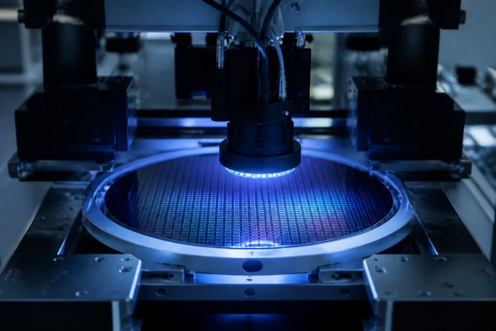
Automated inspection system scanning semiconductor wafers with precision machine vision cameras mounted above wafer handling stage in modern cleanroom environment with blue LED lighting
The return on investment for automated optical inspection depends on production volume, defect rates, and rework costs. For a facility processing 50,000+ wafers monthly, payback typically occurs within 24-30 months. For facilities processing 100,000+ wafers monthly, payback accelerates to 12-18 months.
Here’s how the calculation works: Start with annual labor savings. A facility eliminating 10 manual inspection positions saves $600,000-$750,000 in direct labor annually. Add reduced rework costs from improved defect detection. If manual inspection misses defects that later cause yield loss, automated systems catch those defects earlier, preventing costly rework. Many facilities see rework cost reductions of $200,000-$500,000 annually from improved detection accuracy.
Against these savings, subtract annual operating expenses for the automated system: maintenance contracts, software licensing, and occasional component replacement typically total $80,000-$150,000 annually. The net annual benefit often reaches $750,000-$1.1 million for high-volume operations.
Divide the capital investment ($1 million average) by annual net benefit ($900,000 average), and you get a payback period of approximately 13 months. This calculation assumes steady-state production and doesn’t account for additional benefits: improved yield, reduced cycle time, and better process control that drive incremental revenue.
What complicates ROI analysis is the defect catch rate improvement. If your manual inspection process currently misses 15-20% of defects, and those defects cause wafers to fail downstream (costing $500-$2,000 per wafer in rework or scrap), the automated system’s improved detection directly prevents that loss. For a facility processing high-value wafers, this benefit alone can justify automation investment in under 12 months. AI automation pricing models.
Automated optical inspection directly improves semiconductor yield by catching defects earlier in the production process. Early detection means defective wafers are segregated before expensive processing steps occur, reducing rework costs and preventing yield-killing defects from propagating downstream.
The yield improvement mechanism works in stages. First, automated systems detect surface defects and pattern anomalies that manual inspection misses. Second, consistent defect reporting enables process engineers to identify root causes and adjust process parameters. Third, real-time defect feedback allows production teams to make mid-run corrections before entire batches become scrap.
Many facilities see yield improvements of 2-5% within the first year of automated inspection deployment, depending on their baseline yield and process maturity. For a facility producing 100,000 wafers monthly with a baseline yield of 88%, a 3% improvement means 3,000 additional good wafers monthly, worth $1.5 million to $3 million annually in incremental revenue (depending on wafer value).
The yield improvement also feeds back into cost reduction. Higher yields mean lower per-wafer manufacturing cost, which improves gross margins and competitive positioning. This is why automated optical inspection ROI analysis must account for both cost savings and revenue improvement, the combined effect often exceeds initial projections.
Hybrid approaches can accelerate yield improvements further. Some facilities use automated systems for initial high-speed screening, then deploy manual inspection for secondary verification on flagged wafers. This hybrid model captures automation’s speed advantage while preserving human judgment for ambiguous cases. The trade-off is added complexity, but for specialty or low-volume production, hybrid models often balance cost and accuracy better than pure automation or pure manual inspection.
The false choice between full automation and full manual inspection obscures a more nuanced reality: many facilities operate hybrid models that combine automated screening with selective manual verification. A hybrid approach uses automated optical inspection to rapidly scan every wafer, then routes flagged wafers to manual inspection for human judgment on ambiguous defects.
This strategy captures automation’s speed advantage, processing 200+ wafers per hour, while preserving human technicians for the 5-10% of wafers that require detailed analysis. The result is throughput approaching full automation with labor costs significantly lower than pure manual inspection. A facility processing 100,000 wafers monthly might run automated screening 24/7 (requiring minimal operator attention) and employ 2-3 technicians for secondary verification, reducing total labor cost to $150,000-$200,000 annually versus $1.5 million for full manual inspection.
TCO analysis reveals where hybrid models excel by accounting for all cost categories over a 5-year ownership period, not just capital and labor. TCO includes:
1. Capital Expenditure (Year 1)
2. Annual Labor Costs (Years 1-5)
3. Maintenance and Support (Years 1-5)
4. Energy and Facility Overhead (Years 1-5)
5. Training and Skill Development (Years 1-5)
6. Rework and Yield Loss (Years 1-5)
7. Downtime and Contingency (Years 1-5)
For a facility processing 100,000 wafers monthly:
Full Automation TCO (5 years):
Hybrid Model TCO (5 years):
Full Manual TCO (5 years):
Wait, why does manual appear cheapest? This example assumes your manual inspection process is already mature and your yield loss from missed defects is already baked into your cost structure. If you’re currently losing $300K-$800K annually to rework from missed defects, full automation or hybrid actually delivers higher savings. The TCO comparison shifts dramatically when you account for the true cost of defect misses.
Hybrid models deliver the lowest TCO for mid-volume facilities (20,000-50,000 wafers monthly) because they:
For a facility with 30,000 wafers monthly, a hybrid model might run automated screening 12 hours daily (processing 2,400-3,000 wafers) and employ 2 technicians for secondary verification and manual overflow. This configuration costs roughly $1.2M in capital (lower than full automation) and $200K-$250K annually in labor, delivering a 3-4 year payback period.
A critical challenge in hybrid models is ensuring consistency between automated and manual defect detection. If the automated system flags a defect as “pattern anomaly” but the technician disagrees, which judgment prevails? Applied Physics calibration wafer standards address this by providing reference wafers with known defects that both the automated system and manual technicians can validate against. This cross-validation ensures your hybrid model maintains consistent defect detection across both pathways and prevents defect classification drift over time.
The hybrid approach also mitigates risk. Full automation requires significant capital investment and process integration; if the system underperforms or requires unexpected maintenance, production halts. Manual inspection is slower but resilient; if one technician is absent, you can adjust. Hybrid models balance these concerns: automated systems handle routine screening, and manual technicians provide backup and handle edge cases, creating operational redundancy that pure automation cannot offer.
The decision to automate wafer inspection hinges on four factors: production volume, wafer complexity, defect density, and capital availability. Here’s a practical framework.
Automate if: You’re processing 50,000+ wafers monthly, your wafers have sub-28nm features requiring high defect detection sensitivity, your baseline yield is below 92%, or your current manual inspection labor cost exceeds $800,000 annually. At these thresholds, automation’s payback period compresses to 18-24 months, making the investment clearly justified.
Consider hybrid if: You’re processing 20,000-50,000 wafers monthly, your wafers are mid-complexity (28nm-90nm), your yield is stable (92-96%), or you have variable production volume. Hybrid models give you automation’s throughput advantage with lower capital risk and labor flexibility.
Maintain manual if: You’re processing under 20,000 wafers monthly, your wafers are specialty or low-volume, or your capital budget is constrained. Manual inspection’s low upfront cost and flexibility make it optimal for small operations. The per-wafer cost is higher, but total annual cost remains lower than automation.
This decision should also account for your facility’s process maturity and defect profile. If you’re still optimizing process parameters and defect sources are unstable, manual inspection’s flexibility and lower capital commitment may be preferable while you stabilize. Once your process is mature and defect patterns are consistent, automation becomes more valuable because the system can be reliably calibrated to your specific defect signatures.
Consider also the trajectory of your business. If you’re growing toward higher volumes, starting with hybrid inspection positions you to scale to full automation without stranding capital. If your production is stable or declining, manual inspection’s lower fixed cost makes more sense.
One final consideration: regulatory and quality requirements. If you operate under strict GMP or ISO compliance regimes (as pharmaceutical and medical device manufacturers do), automated inspection’s perfect repeatability and audit trail create compliance advantages that offset some capital cost. Manual inspection requires extensive documentation and technician qualification; automated systems provide objective, machine-readable defect records that satisfy regulatory scrutiny more easily.
The decision between automated and manual wafer inspection cost ultimately depends on your production scale, defect complexity, and financial runway. For most high-volume semiconductor facilities, automation’s superior defect detection and throughput justify the capital investment within 24 months. For smaller operations, hybrid models or manual inspection remain economically sound. Applied Physics helps facilities validate this decision by providing calibration wafer standards that ensure your chosen inspection method, whether automated, manual, or hybrid, maintains the defect detection accuracy and dimensional precision required for consistent yield and GMP compliance. Contact Applied Physics to discuss which inspection strategy aligns with your production requirements and cost targets.
Labor represents the largest ongoing cost in manual wafer inspection, with technicians requiring specialized training and working in controlled cleanroom environments. Automated systems shift costs to capital equipment and maintenance but eliminate recurring labor expenses. For high-volume production running 24/7, automation typically achieves lower per-wafer inspection costs within 18-36 months. The break-even point depends on production volume, wafer complexity, and defect detection requirements specific to your node size and process control standards.
Manual inspection relies on human judgment and subjective analysis, with detection rates typically 85-92% for surface defects and pattern errors. Automated optical inspection systems achieve 95-99% consistency using machine vision and dimensional accuracy measurements. Automated systems eliminate human fatigue and detect sub-micron defects across 300mm, 200mm, and smaller wafers consistently. However, automated systems may generate false positives on certain defect types, requiring fine-tuning for specific process nodes and defect signatures in your cleanroom environment.
Most semiconductor facilities see positive ROI within 24-36 months, depending on production volume and labor costs. Facilities running 200+ wafers daily typically break even faster than lower-volume operations. The calculation includes capital expenditure for equipment, installation, training, and integration with existing metrology and process control systems. Energy and facility overhead costs are lower with automation, but rework and false positive management must be factored into the total cost of ownership analysis for accurate payback projections.
Yes. Many semiconductor manufacturers use hybrid models: automated systems for high-volume, routine inspection of standard defect types, paired with manual inspection for complex pattern errors or new process nodes requiring subjective analysis. This approach balances capital expenditure with labor flexibility and maintains high defect catch rates. Hybrid models work well for facilities transitioning to smaller node sizes or managing multiple wafer sizes (300mm, 200mm, 150mm). The key is identifying which inspection tasks benefit most from automation based on your yield management goals and contamination risk profile.
APPLIED PHYSICS TECHNICAL RESOURCE
Wafer inspection, SSIS calibration, particle deposition references, process control and semiconductor measurement workflows. Product and standards references should be interpreted for the actual instrument, facility, protocol and configuration.

Enter your details below to save your shopping cart for later. And, who knows, maybe we will even send you a sweet discount code :)
Allow notifications to get real-time updates about your shopping cart and who knows, you may even receive a sweet discount code 😊