Last Updated: August 24, 2026
Semiconductor manufacturing standards are technical specifications and protocols that define how semiconductor devices, equipment, materials, and processes must be designed, tested, and operated to ensure product quality, safety, and environmental compliance. These standards span equipment automation, cleanroom environments, metrology, safety protocols, and data acquisition frameworks that manufacturers must follow to produce reliable chips at scale.
The semiconductor industry relies on standardized approaches because the stakes are extraordinarily high. A single defect in a wafer can render thousands of chips unusable. Contamination in a cleanroom can cascade into yield losses across entire production runs. Without unified standards, manufacturers would operate in isolation, unable to share best practices or ensure interoperability between equipment from different vendors. Standards create a common language that allows the industry to advance collectively.
Applied Physics has spent more than three decades supporting manufacturers navigating these complex requirements. The company’s calibration wafer standards and cleanroom monitoring systems help facilities maintain the precision control that semiconductor manufacturing demands. Understanding which standards apply to your operation, and how to implement them effectively, is the foundation of operational excellence in this industry.
Semiconductor manufacturing standards exist for three critical reasons: they reduce defect rates and improve yield, they ensure equipment and systems can work together seamlessly, and they protect worker safety and environmental integrity. Without these standards, manufacturers would face unpredictable quality outcomes, incompatible equipment ecosystems, and regulatory exposure.
Yield optimization is the first driver. A semiconductor fab producing 300mm wafers at advanced nodes can lose millions of dollars per day if contamination or process drift goes undetected (semi.org). Standards for metrology, calibration, and process control give manufacturers the tools to catch problems before they propagate through production. When a calibration wafer standard confirms that your measurement equipment is reading accurately, you can trust that downstream process adjustments are based on real data, not instrument drift.
Interoperability is the second reason standards matter. Modern semiconductor fabs use equipment from multiple vendors: deposition tools from one manufacturer, etch systems from another, lithography platforms from a third. SEMI standards like SECS/GEM (Semiconductor Equipment Communications Standard/Generic Equipment Model) define how these systems communicate and share data. Without this standardization, integrating new equipment into an existing line would require custom engineering for each interface. With standards, a new tool can connect to the fab’s data network and start contributing to the manufacturing intelligence system immediately.
The third driver is regulatory and occupational health compliance. Semiconductor manufacturing involves hazardous materials, photoresists, etchants, dopants, and process gases. Standards for equipment automation, cleanroom protocols, and emission control ensure that workers are protected and environmental contamination is minimized. Standards also create an audit trail that satisfies regulatory bodies and demonstrates that your facility operates with deliberate control.
Semiconductor metrology standards define how to measure critical dimensions, particle contamination, and material properties with the precision required at advanced nodes. These standards ensure that measurement equipment itself is calibrated correctly, so that process decisions based on those measurements are sound.
The core metrology challenge is this: as feature sizes shrink toward 3nm and below, the margin for error shrinks with them. A 5nm process node requires measurement uncertainty well below 1nm. Achieving this requires not just precise instruments, but also reference standards, calibration wafers that have been characterized to known specifications, and documented procedures for how measurements are taken and interpreted.
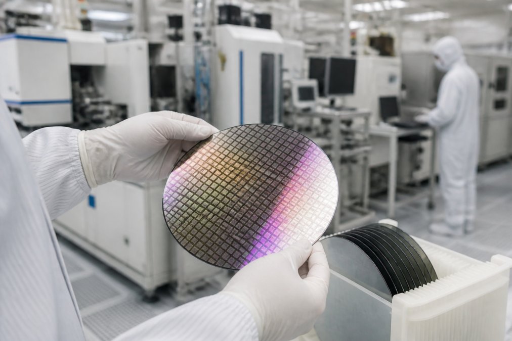
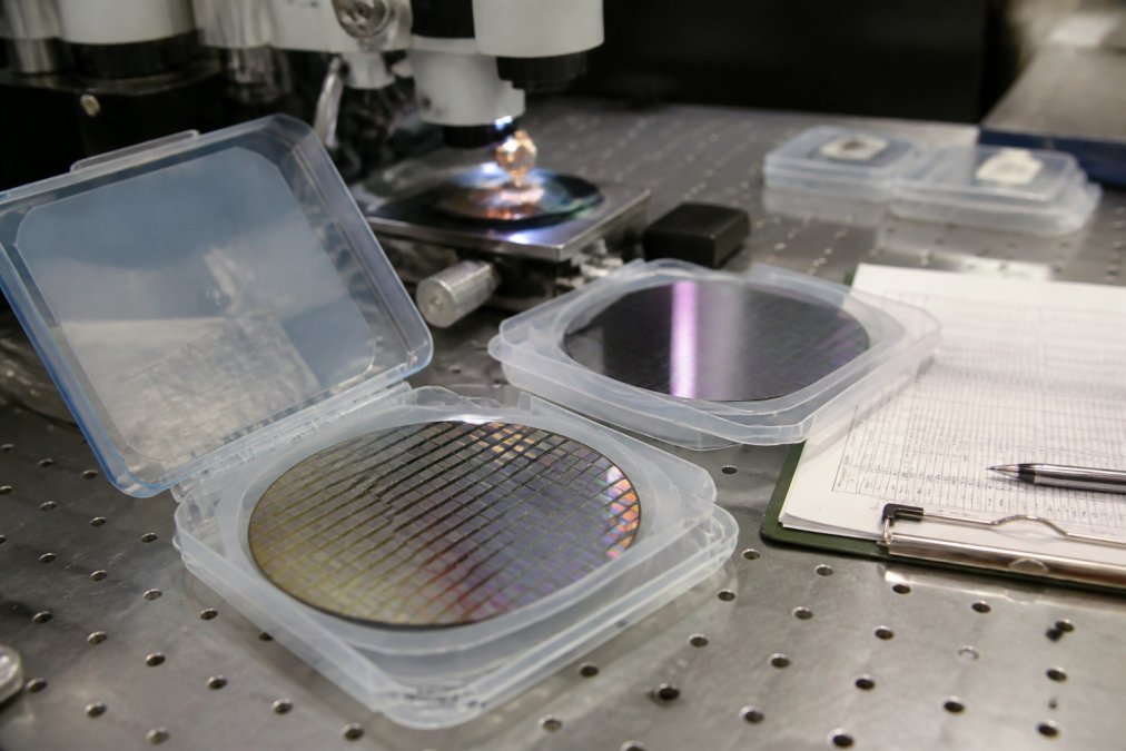
Calibration wafer standards serve as the foundation of metrology confidence. These reference artifacts are manufactured to exact specifications and measured with traceable equipment to establish their true dimensions and properties. When your in-fab measurement tool reads a calibration wafer, you can compare the tool’s reading to the wafer’s certified value. If they match within tolerance, your tool is calibrated. If they drift, you’ve detected instrument drift before it corrupts your process data.
Applied Physics provides calibration wafer standards across multiple wafer sizes, 125mm, 150mm, 200mm, and 300mm, to support different fab configurations. These standards are characterized for dimensional accuracy, uniformity, and repeatability, allowing manufacturers to validate that their metrology equipment is performing within specification.
Particle metrology standards address another critical measurement domain. Cleanroom environments must maintain particle counts within specified limits. Standards define particle size thresholds, counting methodologies, and acceptable contamination levels for different process areas. A semiconductor fabrication facility might require fewer than 100 particles larger than 0.5 micrometers per cubic foot in the most critical areas. Validating that your particle counting equipment is accurate requires reference standards and calibration procedures.
SEMI S2 is a foundational standard that defines safety requirements for semiconductor manufacturing equipment. The standard covers hazard identification, risk assessment, protective measures, and documentation requirements that equipment manufacturers and fab operators must follow.
SEMI S2 establishes that equipment designers must identify all hazards associated with their systems, mechanical, electrical, thermal, chemical, and operational hazards. For each hazard, the standard requires that designers implement protective measures in a defined hierarchy: eliminate the hazard if possible, reduce the risk through design, provide guards and interlocks, and finally, provide warnings and training.
For fab operators, SEMI S2 compliance means ensuring that all equipment in your facility meets these safety specifications and that your maintenance and operational procedures preserve those safety features. This includes regular inspection of interlocks, emergency stop systems, and chemical handling protocols. Equipment that doesn’t meet SEMI S2 standards creates liability exposure and increases the risk of worker injury.
The standard also requires that equipment documentation, manuals, maintenance procedures, spare parts specifications, be clear and complete. When a technician needs to service a tool, they should be able to follow documented procedures that ensure safety throughout the maintenance process. SEMI S2 compliance verification is often part of regulatory audits and customer qualification processes.
Calibration wafer standards are precision reference artifacts used to validate that in-fab measurement equipment is operating within specification. They’re essential for yield optimization because they create a traceable link between your process measurements and absolute physical reality.
Here’s how the chain of traceability works: a calibration wafer is manufactured to exact specifications and measured with equipment that itself is traceable to national standards maintained by NIST (National Institute of Standards and Technology). Your fab receives this wafer with a certificate stating its dimensional properties. You then measure the same wafer with your in-fab tools and compare your readings to the certified values. If your tool reads within tolerance, you can trust that all subsequent measurements made with that tool are accurate. If your tool reads outside tolerance, you know the tool needs recalibration before it can be used for process control.
For semiconductor manufacturing, this traceability is non-negotiable. Process engineers make decisions about etch depth, film thickness, and linewidth based on metrology data. If that data is corrupted by instrument drift, the decisions are wrong, and yield suffers. A single wafer lot that’s been processed with incorrect metrology data can represent hundreds of thousands of dollars in scrap.
Calibration wafer standards come in different configurations depending on what you need to measure. Some standards are optimized for dimensional metrology, measuring the width and depth of features. Others are designed for overlay measurement, ensuring that different layers of a chip align correctly. Still others are used for resist uniformity validation or photomask inspection.
Applied Physics calibration wafer standards are available in 125mm, 150mm, 200mm, and 300mm formats to match your fab’s wafer size portfolio. Each standard is characterized for the specific measurement domain it serves, with documented specifications and uncertainty budgets.
Cleanroom environments are the physical foundation of semiconductor manufacturing. The air inside a cleanroom is filtered continuously to remove particles, and the space is maintained at positive pressure so that unfiltered air cannot infiltrate. Cleanroom protocols define the design standards, operating procedures, and validation methods that keep contamination below acceptable levels.
ISO 14644 is the international standard that defines cleanroom classifications based on particle count limits. An ISO Class 3 cleanroom, the strictest classification, allows no more than 35 particles larger than 0.5 micrometers per cubic foot of air. An ISO Class 5 cleanroom, which is common in semiconductor fabs, allows up to 3,520 such particles per cubic foot (iso.org). These classifications sound abstract until you consider that a single human hair is about 75 micrometers in diameter, and a fingerprint can deposit millions of particles onto a surface.
Maintaining these particle counts requires continuous operation of HEPA (High Efficiency Particulate Air) filters, positive pressure differentials between cleanroom zones, and strict protocols for personnel entry and material handling. Gowning procedures, the process of putting on protective equipment before entering the cleanroom, are standardized to minimize the introduction of particles from street clothes.
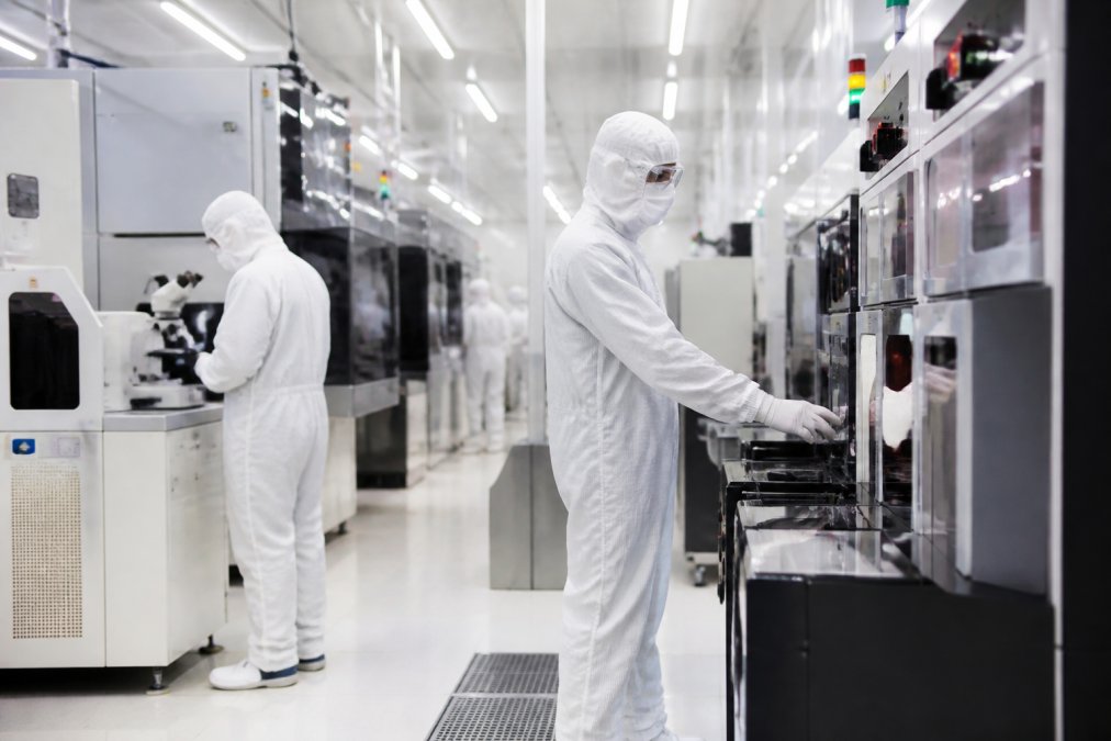
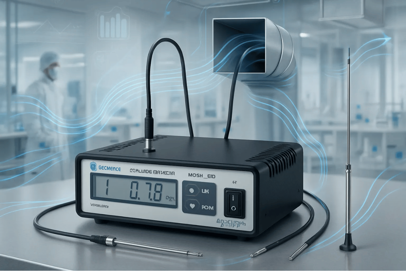
Airflow visualization is a critical validation tool for cleanroom performance. Smoke or fog introduced into the cleanroom allows operators to see how air moves through the space, identify dead zones where particles might accumulate, and confirm that the ventilation system is creating the intended flow patterns. Applied Physics provides cleanroom foggers that generate consistent fog for airflow validation studies. Many facilities use these tools during initial qualification and then periodically during maintenance or equipment changes to confirm that airflow patterns remain optimal.
Equipment placement within the cleanroom is also standardized. Tools that generate particles or heat must be positioned to minimize their impact on the cleanroom environment. Air handling units and filter banks are typically located above work areas, and return air is drawn from the lower portions of the cleanroom, creating a top-to-bottom airflow pattern that sweeps particles toward exhaust points.
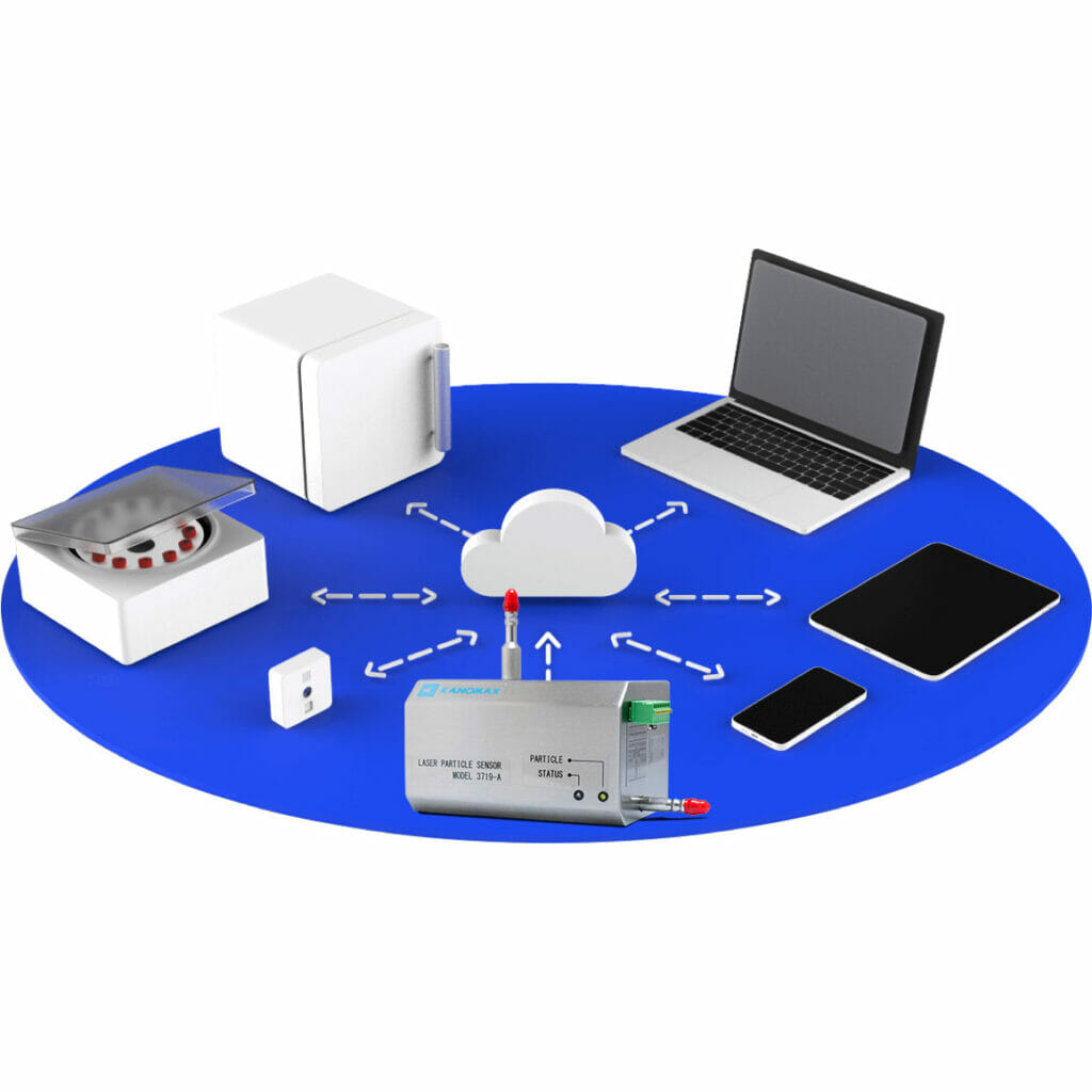
Equipment automation standards define how semiconductor manufacturing tools communicate with each other and with the fab’s manufacturing execution system (MES). These standards enable data to flow continuously from equipment sensors to process control systems, creating the visibility needed for real-time optimization and predictive maintenance.
SEMI SECS/GEM (Semiconductor Equipment Communications Standard / Generic Equipment Model) is the foundational standard for equipment integration. SECS/GEM defines a message format and protocol that allows different equipment vendors’ tools to exchange data in a standardized way. The standard specifies how tools report their status, receive commands, stream process data, and log events. Without this standard, each new tool would require custom software bridges to connect to the fab’s data network, a process that could take weeks or months and cost hundreds of thousands of dollars. With SECS/GEM, a tool manufacturer implements the standard protocol once, and the tool can connect to any fab’s MES that also supports the standard.
The SECS/GEM protocol operates in layers. The message layer (SECS) defines the structure of data being exchanged: equipment status, alarm conditions, process parameters, and equipment diagnostics. The equipment model layer (GEM) defines the state machines and transitions that govern how equipment behaves in response to commands and how it reports its condition. For example, a deposition tool might transition from "Idle" to "Processing" when the MES sends a recipe command, and it must report its state and any alarms back to the MES at defined intervals.
The hardware interfaces that implement SECS/GEM have evolved significantly. Older implementations used serial connections (RS-232 or RS-485) with baud rates of 9,600 to 19,200 bits per second, adequate for status updates but too slow for continuous sensor streaming. Modern implementations use Ethernet with TCP/IP, supporting data rates of 100 megabits per second or higher. This evolution has enabled the transition from periodic data polling (asking equipment for status every few seconds) to continuous streaming of sensor data (temperature, pressure, gas flow rates, power consumption) at rates of 10-100 samples per second.
GEM300 is an extension of SECS/GEM that adds capabilities for real-time process data collection and equipment diagnostics. A tool compliant with GEM300 can stream continuous sensor data to the fab’s data acquisition system without overwhelming the network. The standard defines how data is time-stamped, what metadata accompanies each reading (which sensor, what units, what range), and how the tool handles data buffering if the network is temporarily unavailable. This streaming data enables predictive maintenance (detecting when a component is beginning to fail before catastrophic failure occurs) and advanced process control (adjusting tool parameters in real time based on measured outcomes).
Implementation challenges are common, especially for smaller manufacturers integrating legacy equipment. Older tools may not have been designed with SECS/GEM in mind, requiring retrofitting with new control electronics or software bridges. These bridges translate between the tool’s native communication protocol and SECS/GEM, but they introduce latency and potential data loss. A fab integrating a 15-year-old lithography tool might need to install a gateway device that polls the tool every 500 milliseconds and translates its proprietary status messages into SECS/GEM format. This approach works but introduces a 250-millisecond average delay in data delivery.
Equipment automation also encompasses safety interlocks and emergency stop systems. These systems must operate reliably and independently of the main process control logic. A tool’s emergency stop button must halt all hazardous operations immediately, regardless of what the MES is commanding. Standards for equipment automation ensure that safety-critical functions are designed and validated separately from process control functions. SEMI S2 and related standards specify that emergency stop circuits must be hardwired, not software-controlled, so that a software failure cannot prevent an emergency stop from working.
Data validation is a critical but often overlooked aspect of equipment automation. When a tool reports that its chamber temperature is 500 degrees Celsius, the MES must validate that this reading is physically plausible for the current process step. If a tool reports a temperature of 5,000 degrees Celsius, that’s clearly an instrument failure or data corruption, not a real condition. Standards define validation rules and error handling procedures. If a reading fails validation, the system logs an error, alerts operators, and may halt the process to prevent bad data from corrupting process control decisions.
For smaller manufacturers, SECS/GEM compliance is increasingly a customer requirement. Large chip designers and foundries specify that their suppliers’ equipment must support SECS/GEM so that data can flow seamlessly when tools are installed at customer sites. This creates a practical incentive for equipment vendors to implement the standard, even though the upfront engineering cost is significant. A specialty fab that wants to serve these customers must ensure that its equipment, whether newly purchased or retrofitted, supports SECS/GEM communication.
SECS/GEM enables the continuous flow of data from equipment to the fab’s information systems, but standards for data acquisition and analytics determine how that data is organized, validated, and used for decision-making. These frameworks transform raw sensor streams into actionable intelligence.
The data acquisition layer begins with sensors on equipment, temperature probes, pressure transducers, flow meters, particle counters. These sensors generate continuous streams of readings. Standards define how these readings are time-stamped, validated for reasonableness, and transmitted to the data collection system. A reading that’s physically impossible (e.g., a temperature of 5,000 degrees Kelvin) is flagged as invalid rather than incorporated into the analysis.
Once data is collected, analytics frameworks apply process control algorithms to detect drift, predict failures, and optimize outcomes. Statistical process control (SPC) is a foundational framework that uses control charts to distinguish between normal process variation and out-of-control conditions. When a process metric drifts outside control limits, the system alerts operators so they can investigate and correct the root cause before yield is impacted.
Advanced analytics frameworks layer machine learning on top of traditional SPC. These systems can identify subtle patterns in sensor data that precede failures or quality issues. A tool’s bearing might begin to degrade weeks before catastrophic failure; machine learning models trained on historical data can detect the early warning signs in vibration and temperature patterns.
Data governance standards ensure that data is accurate, traceable, and secure. Every data point should be associated with the equipment that generated it, the time it was collected, and the person or system that accessed it. This traceability is essential for regulatory compliance and for root cause analysis when problems occur.
Semiconductor manufacturing generates hazardous air pollutants and wastewater that must be managed to protect environmental and worker health. Standards for environmental compliance define allowable emission limits, monitoring requirements, and control technologies.
The EPA’s National Emission Standards for Hazardous Air Pollutants (NESHAP) apply to semiconductor manufacturing facilities. These standards limit emissions of volatile organic compounds (VOCs), fluorinated greenhouse gases, and other hazardous substances. Facilities must install emission control equipment, scrubbers, thermal oxidizers, or other systems, to reduce emissions below the NESHAP limits.
Monitoring is a critical compliance requirement. Facilities must measure their emissions continuously or periodically, depending on the substance and the specific NESHAP regulation. This monitoring data is reported to the EPA and becomes part of the regulatory record. Inaccurate monitoring can result in violations and penalties.
Wastewater treatment standards address the chemical effluents generated during semiconductor manufacturing. Processes like chemical mechanical polishing (CMP), photoresist stripping, and metal etching produce wastewater containing heavy metals, organic compounds, and other contaminants. Standards define treatment processes and discharge limits that ensure wastewater can be safely released to municipal treatment systems or disposed of properly.
Hazardous waste management standards govern how chemical byproducts are stored, labeled, transported, and ultimately disposed of. A semiconductor fab generates hazardous waste continuously, spent photoresist, contaminated cleaning solutions, and other process byproducts. These materials must be segregated, containerized, and tracked according to EPA and state regulations.
Worker safety in semiconductor manufacturing is governed by OSHA (Occupational Safety and Health Administration) standards and industry-specific guidelines. However, semiconductor fabs face hazards that differ significantly from other manufacturing environments: exposure to highly toxic process gases, corrosive chemicals, cryogenic liquids, and the combination of these hazards in confined spaces. Standards and regulations address these unique risks through a hierarchy of controls that prioritizes elimination and substitution over personal protective equipment.
Chemical safety is paramount because semiconductor manufacturing uses substances that are acutely toxic at very low concentrations. Phosphine (PH₃) is used in doping processes and is lethal at concentrations above 200 parts per million (the CDC). Silane (SiH₄) is used in deposition and is flammable and toxic. Hydrofluoric acid (HF) is used in etching and is corrosive and highly toxic; skin contact with HF can cause systemic fluoride poisoning and cardiac arrest. Arsine (AsH₃) and diborane (B₂H₆) are used in ion implantation and are extremely toxic. These gases require specialized handling, storage, and detection systems.
OSHA’s Process Safety Management (PSM) standard (29 CFR 1910.119) requires facilities that handle hazardous chemicals above threshold quantities to establish comprehensive safety programs. For semiconductor fabs, this means:
Hazard Analysis: Facilities must conduct Process Hazard Analyses (PHAs) that identify all potential failure modes in chemical handling systems. A PHA for a silane delivery system, for example, would consider what happens if a regulator fails, if a line ruptures, if a check valve leaks, or if pressure relief systems malfunction. For each failure mode, the analysis identifies the consequences and the safeguards that prevent or mitigate the failure.
Safe Operating Procedures: PSM requires written procedures for normal operations, startup, shutdown, and emergency response. These procedures must specify the sequence of steps, the equipment to be used, the parameters to be monitored, and the actions to take if parameters drift outside acceptable ranges. A procedure for phosphine delivery might specify that operators must verify gas purity before connecting a cylinder, that they must check pressure gauges at specified intervals, and that they must immediately isolate the system if pressure exceeds a defined threshold.
Mechanical Integrity: Equipment used in hazardous chemical service must be designed, installed, maintained, and inspected according to engineering standards. Pressure vessels, piping, regulators, and relief systems must meet ASME (American Society of Mechanical Engineers) standards. Facilities must establish inspection and testing schedules; for example, pressure relief devices might be tested annually, and piping systems might be inspected for corrosion every two years.
Training and Competency: All personnel who work with hazardous chemicals must receive training on the hazards, the safe handling procedures, the emergency response procedures, and the location of safety equipment. This training must be documented and repeated periodically or when procedures change. New employees typically receive 8-16 hours of initial training before they are allowed to work with hazardous chemicals independently.
Management of Change: When a facility modifies a process, changes equipment, or introduces a new chemical, PSM requires a formal change management process. The change must be evaluated for its impact on safety, and all affected procedures, training, and equipment inspections must be updated. A change as seemingly minor as switching from one supplier’s phosphine to another supplier’s phosphine requires evaluation because the new supplier’s purity specifications or cylinder pressure ratings might differ.
The control hierarchy for chemical hazards prioritizes elimination and substitution above all else. If a process can be redesigned to eliminate a hazardous chemical, that is the preferred approach. If elimination is not feasible, substitution with a less hazardous chemical is the next preference. Only when elimination and substitution are not feasible do facilities implement engineering controls (ventilation, containment, automated handling) and administrative controls (procedures, training, monitoring). Personal protective equipment is the last line of defense, not the primary control.
For example, consider a photoresist stripping process that traditionally used a highly toxic solvent. A facility might redesign the process to use a less toxic solvent, reducing the hazard. If that’s not feasible, the facility might install a closed-loop system where the solvent is automatically dispensed and recovered, minimizing worker exposure. If that’s not feasible, the facility might require workers to wear respirators and work in a ventilated hood. The hierarchy ensures that the most effective controls are implemented first.
Personal protective equipment (PPE) standards define what workers must wear when engineering and administrative controls are insufficient to reduce exposure below acceptable levels. In semiconductor fabs, this includes:
Respirators: Workers handling hazardous gases must wear respirators rated for the specific chemicals in use. A worker handling phosphine must wear a respirator with cartridges rated for phosphine; a respirator rated for organic vapors will not protect against phosphine. OSHA requires that facilities conduct fit testing to ensure that respirators seal properly on each worker’s face. Fit testing is performed annually or whenever a worker’s facial features change significantly (weight loss, dental work, etc.). A respirator that doesn’t fit properly provides little protection because contaminated air can leak around the edges.
Chemical-Resistant Gloves: Different chemicals require different glove materials. Nitrile gloves protect against many organic chemicals but not against hydrofluoric acid; HF requires neoprene or butyl rubber gloves. Glove selection must be based on the specific chemicals in use, and workers must be trained on which gloves to use for which chemicals.
Face Shields and Eye Protection: Many semiconductor processes generate aerosols or splashes. Face shields and chemical splash goggles protect eyes and face. Standards specify the impact resistance and chemical compatibility of eye protection.
Protective Clothing: Workers handling hazardous chemicals often wear chemical-resistant aprons, sleeves, or full-body suits depending on the hazard level. Clothing must be selected to protect against the specific chemicals in use and must be inspected regularly for tears or degradation.
Emergency response procedures must be established and practiced. Facilities must maintain spill response kits containing absorbent materials, neutralizing agents, and containment equipment appropriate to the chemicals in use. Emergency eyewash and shower stations must be located within 10 seconds of any area where hazardous chemicals are handled. These stations must be tested weekly to ensure they function properly. Trained personnel must be available to respond to chemical releases, and the facility must conduct drills at least annually to ensure that emergency procedures are understood and can be executed quickly.
Occupational exposure limits (OELs) define the maximum concentration of a hazardous substance that workers can be exposed to without adverse health effects. OSHA establishes Permissible Exposure Limits (PELs); for example, the PEL for phosphine is 0.3 parts per million (ppm) as an 8-hour time-weighted average. Many semiconductor fabs adopt more stringent limits based on industry best practices or customer requirements. Facilities must monitor worker exposure through air sampling, either personal air samplers worn by workers or area samplers placed in work zones. Sampling results are compared to OELs, and if exposure exceeds limits, the facility must investigate the cause and implement corrective actions.
Ergonomic standards address the physical demands of semiconductor manufacturing work. Many tasks, standing at workstations for extended periods, performing repetitive motions, manipulating heavy materials, create risk of musculoskeletal strain. OSHA’s ergonomics guidelines recommend workstation design that minimizes awkward postures, tool design that reduces repetitive strain, and work practice guidelines that include breaks and job rotation. Facilities should conduct ergonomic assessments of high-risk jobs and implement controls such as adjustable workstations, mechanical assists for heavy lifting, and job rotation schedules.
Regulatory compliance is validated through OSHA inspections, which can be triggered by worker complaints, accidents, or routine scheduling. During an inspection, OSHA investigators interview workers, review procedures and training records, observe work practices, and collect air samples. Citations for violations can result in significant penalties; serious violations can result in fines of up to $15,131 per violation (2024 rates). Beyond the financial impact, safety violations damage a facility’s reputation and can result in loss of customer business.
As semiconductor feature sizes approach physical limits, the industry is moving toward three-dimensional integration, stacking multiple die vertically and connecting them with through-silicon vias (TSVs). This approach increases transistor density and performance without shrinking feature size further. However, 3D-IC manufacturing introduces new challenges and requires new standards.
3D-IC standards address die thickness uniformity, TSV geometry and reliability, micro-bump specifications, and interconnect integrity. When die are thinned to 50 micrometers or thinner for stacking, they become fragile and require careful handling and support during processing. Standards define the mechanical specifications and handling procedures that prevent breakage.
Through-silicon vias are narrow vertical connections that must maintain electrical integrity through multiple thermal cycles and mechanical stresses. Standards specify the minimum via diameter, the maximum aspect ratio (depth to width), and the material specifications that ensure vias remain conductive and don’t crack during use.
Micro-bump interconnects connect stacked die to each other. These connections are typically 10-20 micrometers in diameter and must carry current reliably across interfaces that may experience differential thermal expansion. Standards define bump geometry, solder composition, and bonding procedures that ensure reliable interconnection.
Advanced packaging standards also address chiplet integration, the practice of assembling multiple smaller die (chiplets) into a single package. This approach offers flexibility in design and manufacturing but requires standards for chiplet interface specifications, known good die (KGD) criteria, and assembly procedures.
Smaller semiconductor manufacturers and specialty fab operators often face a challenge: comprehensive compliance with all applicable standards requires significant investment in equipment, training, and documentation. The implementation roadmap for SMEs differs from that of large integrated device manufacturers.
Start by identifying which standards are most relevant to your specific operations. If you’re a specialty fab focused on analog or power devices, your critical standards differ from those of a logic fab. If you operate a photomask shop, your standards differ from a wafer fab. Review your customer requirements, regulatory obligations, and industry best practices to prioritize which standards to implement first.
Metrology and calibration should be among your first priorities. Without accurate measurement, you cannot control your process effectively. Establishing a calibration program, acquiring calibration wafer standards, validating your measurement equipment, and implementing periodic recalibration, is foundational. Applied Physics calibration wafer standards are available in sizes that match typical specialty fab configurations, making it practical to establish a traceable metrology program even at smaller scales.
Cleanroom protocols come next. Even a small cleanroom requires proper design, filtration, and validation. Start with ISO 14644 classification appropriate to your process requirements. Validate your cleanroom using airflow visualization studies to confirm that particle counts and airflow patterns meet specification. Applied Physics cleanroom monitoring systems and foggers support this validation process.
Equipment integration and data acquisition can be phased in. Start with basic data collection from your most critical process tools, then expand as your capabilities grow. SECS/GEM compliance enables interoperability with equipment from different vendors, so prioritize equipment that supports these standards.
Safety and environmental compliance requirements are non-negotiable from the start. Implement OSHA-compliant chemical safety programs, emergency response procedures, and worker training immediately. These are regulatory minimums, not optional enhancements.
Documentation is often underestimated. Regulatory bodies, customers, and auditors will ask for evidence that you operate according to standards. Maintain records of equipment qualifications, calibration activities, environmental monitoring, and training. This documentation is your proof of compliance.
As semiconductor manufacturing evolves toward advanced nodes and new applications, standards are emerging to address new challenges. Quantum computing, artificial intelligence accelerators, and advanced photonics are creating new requirements for semiconductor manufacturing.
Quantum computing chips require extraordinary levels of control over qubit properties and interconnects. Emerging standards define specifications for qubit fabrication, cryogenic packaging, and control electronics. These standards are still evolving as the industry gains experience with quantum manufacturing.
AI accelerator chips often use specialized memory architectures and compute elements that differ from traditional logic. Standards for AI chip manufacturing address the unique thermal challenges, reliability requirements, and performance specifications of these chips.
Advanced photonics integration, combining optical and electronic components on the same chip, requires new standards for waveguide geometry, coupling efficiency, and optical alignment. These standards are being developed through industry consortia and will become increasingly important as photonic integration expands.
Chiplet-based systems are driving standardization efforts around chiplet interface specifications and chiplet-to-substrate interconnects. As chiplet design becomes more common, standardized interfaces will enable broader ecosystem participation and reduce integration costs.
Semiconductor manufacturing standards represent decades of collective industry experience distilled into technical specifications that enable reliable, safe, and efficient production. From cleanroom protocols to metrology standards to equipment automation frameworks, these standards create the foundation for manufacturing excellence.
Implementing these standards effectively requires understanding which standards apply to your specific operations, prioritizing implementation based on your business model and customer requirements, and investing in the equipment and procedures that ensure compliance. Applied Physics supports this journey by providing calibration wafer standards that enable precise metrology control, cleanroom monitoring systems that validate environmental compliance, and the technical expertise that comes from serving semiconductor manufacturers for over three decades. Contact Applied Physics to discuss how our precision measurement and contamination control solutions can strengthen your manufacturing standards program and improve your operational outcomes.
A: The primary standards include SEMI specifications (S2 for safety, S8 for equipment interfaces), NIST guidelines for measurement and calibration, EPA environmental regulations (NESHAP for hazardous air pollutants), and SECS/GEM protocols for equipment communication and data acquisition. ISO 14644 defines cleanroom classifications, while IPC standards govern assembly processes. These standards address fabrication environments, equipment automation, metrology, process control, and compliance reporting across the entire semiconductor manufacturing ecosystem.
A: Calibration wafer standards ensure that metrology equipment accurately measures critical dimensions at sub-10nm precision levels. Without proper calibration standards, measurement drift goes undetected, leading to out-of-spec products, yield loss, and costly rework. Calibration wafers provide reference artifacts that validate equipment performance, enabling process engineers to maintain uniformity across wafer lots and detect process drift before defects occur. This directly impacts yield optimization and reduces scrap rates.
A: SEMI S2 is the safety guideline standard for semiconductor equipment, specifying hardware interfaces, electrical safety, and occupational health requirements for fabrication tools. It ensures equipment interoperability across suppliers, reduces workplace hazards, and establishes technical agreements between equipment manufacturers and fab operators. Compliance with S2 prevents equipment failures, protects workers from electrical and chemical hazards, and enables faster equipment qualification during fab startups or technology node transitions.
A: EPA NESHAP regulations require semiconductor manufacturers to monitor and control hazardous air pollutants from stationary sources in fabrication facilities. Compliance involves emission testing, equipment upgrades, and continuous monitoring of air quality. These standards increase operational costs through control equipment and documentation but prevent regulatory fines, facility shutdowns, and environmental liability. Proper compliance also improves worker safety and demonstrates corporate responsibility to stakeholders and regulators.
A: SECS/GEM (Semiconductor Equipment Communications Standard/Generic Equipment Model) enables automated communication between fabrication equipment and manufacturing execution systems. This protocol standardizes data acquisition, allowing big data analytics for process control, yield optimization, and predictive maintenance. SECS/GEM integration reduces manual data entry, improves traceability, and enables real-time process adjustments. It's essential for Industry 4.0 implementations in semiconductor fabs seeking to maximize efficiency and reduce downtime.
A: Smaller manufacturers should prioritize SEMI S2 and ISO 14644 cleanroom standards first, then progressively implement metrology calibration and SECS/GEM protocols. Starting with calibration wafer standards for critical process steps allows phased implementation. Partnering with equipment suppliers who provide pre-qualified systems reduces qualification time. Industry associations and NIST resources offer guidance tailored to mid-size operations seeking to meet standards without overwhelming compliance costs.
A: Standards bodies are developing specifications for quantum device fabrication, including control systems for cryogenic environments and measurement protocols for quantum properties. AI-driven process control standards are emerging through SEMI working groups, addressing machine learning model validation, data quality requirements, and cybersecurity for automated fab systems. These standards remain in development, but early adopters should monitor NIST roadmaps and SEMI committee publications for guidance on integrating AI analytics and quantum manufacturing into existing compliance frameworks.
This article was written using GrandRanker

Enter your details below to save your shopping cart for later. And, who knows, maybe we will even send you a sweet discount code :)
Allow notifications to get real-time updates about your shopping cart and who knows, you may even receive a sweet discount code 😊