
In modern semiconductor manufacturing, the margin for error is measured in nanometers.
As devices shrink and architectures become more complex, the surface conditions of silicon wafers dictate the success or failure of subsequent processing steps.
One of the most critical, yet sometimes overlooked, parameters is surface energy.
Understanding and controlling the surface energy of treated wafers ensures optimal adhesion for coatings, flawless wafer bonding, and uniform photolithography.
This article explores the importance of precision metrology for measuring surface energy, how it works, and why it is indispensable for maximizing yield in semiconductor fabrication.
Surface energy is a measure of the intermolecular forces at the surface of a material. In the context of semiconductor wafers, it defines how wettable or reactive the surface of the wafer is. When a silicon wafer undergoes treatments such as plasma activation, chemical etching, or cleaning, its chemical composition changes.
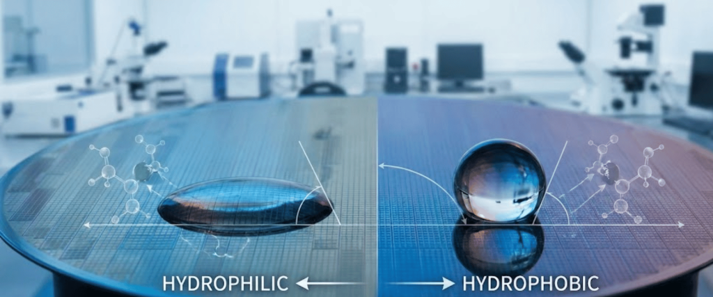
A high surface energy typically means the wafer is highly hydrophilic (water-attracting) and ready to form strong bonds with adhesives, photoresists, or other wafers. Conversely, low surface energy indicates a hydrophobic (water-repelling) surface.
Treating a wafer to achieve a specific surface energy is only half the battle; verifying that the treatment was uniform and successful requires precision metrology.
Failing to measure and control surface energy accurately can lead to severe manufacturing defects.
Precision metrology removes the guesswork, providing quantitative data to confirm that a wafer is perfectly prepped for the next manufacturing step.
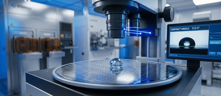
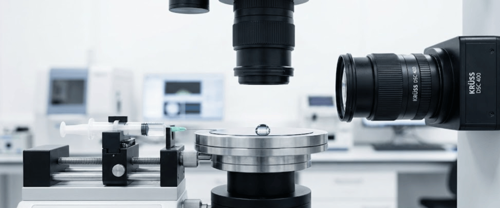
To measure surface energy with high precision, the semiconductor industry primarily relies on advanced contact angle analysis.
The most widespread and accurate method for determining surface energy is measuring the contact angle of a liquid droplet on the wafer’s surface.
By testing the wafer with multiple liquids of known properties, sophisticated software models (like Owens-Wendt-Rabel-Kaelble or OWRK) calculate the exact total surface energy, breaking it down into polar and dispersive components.
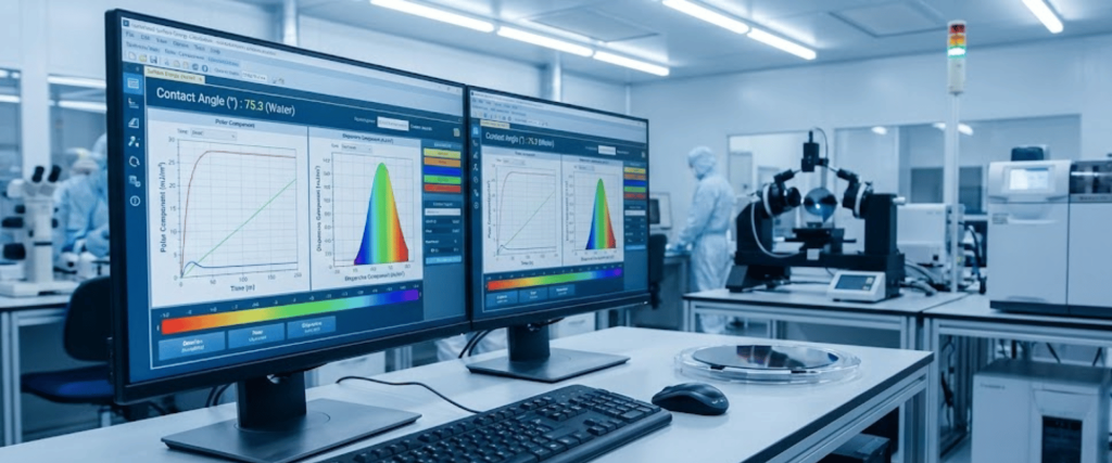
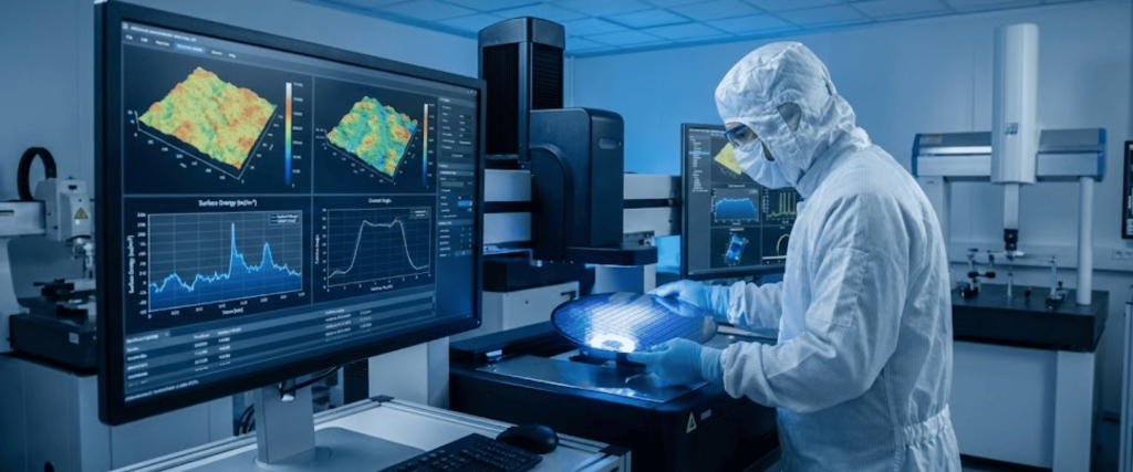
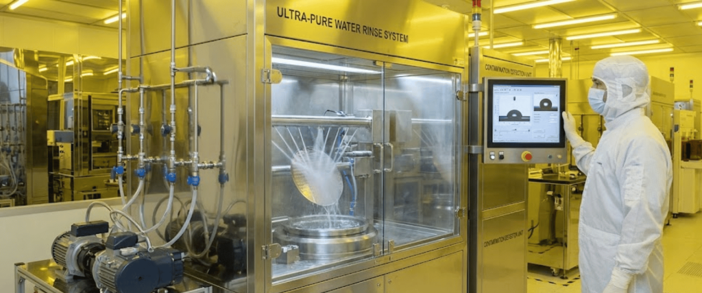
Manual goniometers are insufficient for high-volume manufacturing. Modern precision metrology utilizes fully automated surface analyzers.
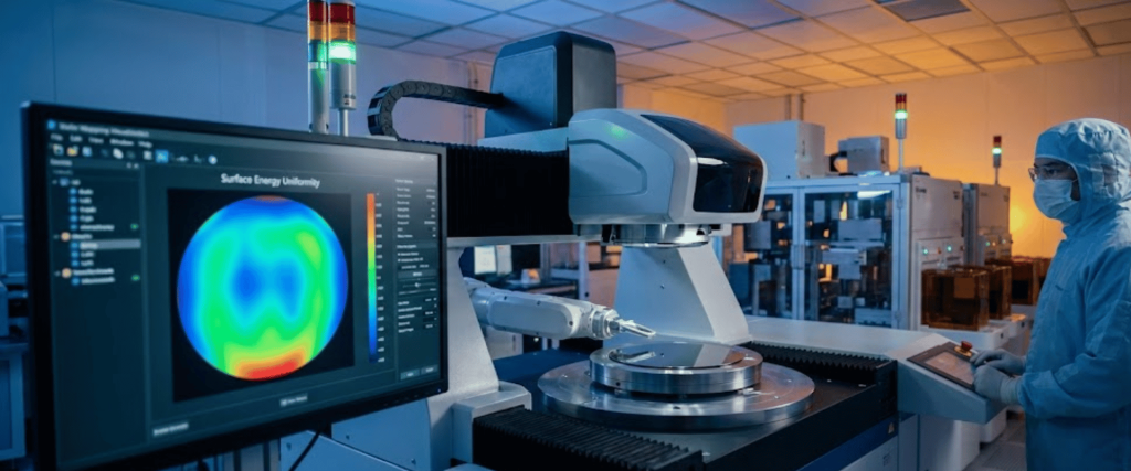
These systems map the entire surface of a 200mm or 300mm wafer, taking dozens of contact angle measurements in seconds to generate a topographical map of surface energy, ensuring edge-to-edge uniformity.
Implementing precise surface energy measurements directly impacts several critical fabrication processes.
In 3D integration and advanced packaging, silicon wafers must be bonded together seamlessly. Before bonding, wafers are typically subjected to plasma activation to maximize surface energy.
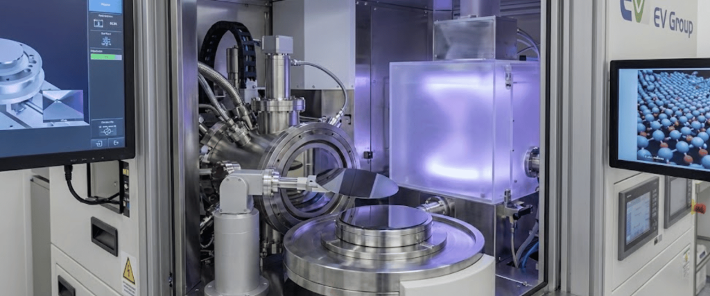
Precision metrology verifies that the plasma treatment was effective across the entire wafer, ensuring strong, void-free covalent bonds.
Photoresist must coat the wafer with absolute uniformity.
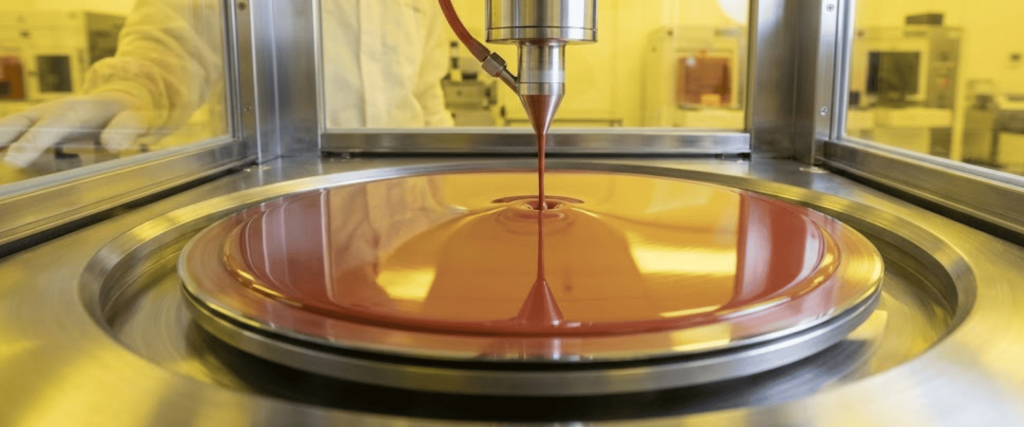
By measuring the surface energy before spin-coating, engineers can guarantee that the resist will wet the surface perfectly, preventing defects during the etching process.
Wafer cleaning steps are designed to remove organic and inorganic contaminants. Measuring the surface energy post-cleaning acts as a highly sensitive cleanliness check.
Even a monolayer of organic contamination will drastically alter the contact angle, alerting quality control to a failing cleaning process.
Investing in precision metrology for surface energy analysis offers significant ROI for fabrication facilities.
As semiconductor architectures push the boundaries of physics, the integrity of every single atomic layer matters.
Precision metrology for measuring the surface energy of treated wafers is no longer a luxury; it is a critical checkpoint for quality control.
By leveraging automated contact angle analysis, fabrication facilities can ensure perfect adhesion, flawless bonding, and ultimately, higher yields in their manufacturing pipelines.
Surface energy defines how wettable or reactive a wafer’s surface is. It directly determines how successfully coatings, photoresists, or other wafers will adhere to the silicon.
The standard method is Contact Angle Goniometry. A precision camera measures the angle of a tiny water or chemical droplet placed on the wafer; a flatter droplet indicates higher surface energy.
Measuring it verifies that the wafer’s surface is perfectly clean and properly activated (usually via plasma). This ensures a strong, uniform bond without microscopic voids, which is essential for advanced packaging.