
Table of Contents
- What Are Semiconductor Wafer Calibration Standards?
- Understanding NIST Traceable Wafer Standards
- PSL Wafer Standards: Polystyrene Latex Particle Deposition
- On-Wafer Calibration Techniques for Semiconductor Devices
- Step-by-Step Calibration Workflow for Semiconductor Manufacturing Quality Control
- Common Calibration Failures and Troubleshooting
- In-House vs. Third-Party Calibration: Cost-Benefit Analysis
- Applications of Calibration Wafer Standards in Semiconductor Production
- Selecting the Right Calibration Wafer Standard for Your Process
- Conclusion
Last Updated: July 29, 2026
What Are Semiconductor Wafer Calibration Standards?
Semiconductor wafer calibration standards establish baseline references that ensure all metrology equipment delivers reproducible, traceable measurements. These standards serve as physical reference objects with known properties. When your inspection equipment measures a calibration wafer, it should report values matching the certified specifications. If numbers diverge, your equipment needs adjustment or maintenance.
A single undetected measurement error in a 300mm fab can invalidate thousands of wafers. Particle counts might appear acceptable when unsafe. Thin film thickness might read correct when out of spec. The financial and safety implications are enormous.
The most overlooked aspect of calibration standards is documentation. Keep detailed records of every calibration event, date, equipment used, ambient conditions, and results. This traceability chain becomes essential during audits and when troubleshooting measurement inconsistencies months later.
Understanding NIST Traceable Wafer Standards
NIST traceability means your calibration wafer connects to the National Institute of Standards and Technology through an unbroken chain of documented measurements. This is the foundation of compliance in regulated industries.
When a wafer carries NIST certification, metrologists have measured it using reference standards traceable to NIST, with documented measurement uncertainty. Your equipment, when calibrated against that wafer, inherits that same traceability. This chain matters because regulators, auditors, and customers all expect it.
The traceability documentation includes the certificate of calibration specifying exact measurements (particle size distribution, count per unit area, thin film thickness), the measurement uncertainty range, and the standards used to certify the wafer with their own NIST connection. According to NIST guidance on measurement traceability, measurement uncertainty must be quantified and communicated, without it, your calibration is essentially worthless in a regulated environment.
Applied Physics calibration wafers come with full NIST traceability documentation. When you receive a calibration wafer standard from Applied Physics, the certificate includes measurement results, uncertainty statements, and the complete traceability chain back to NIST.
PSL Wafer Standards: Polystyrene Latex Particle Deposition
Polystyrene latex (PSL) spheres represent the gold standard for particle calibration in semiconductor manufacturing. These uniform, spherical particles of known size are deposited onto wafers in precise patterns.
PSL particles are monodisperse, every particle in a batch has virtually identical size and density. They’re stable over time and don’t react with water or solvents. For metrology systems verifying particle detection accuracy, PSL wafers are the reference standard.
Manufacturers suspend PSL spheres in a carrier liquid, then deposit them onto clean wafer surfaces using specialized equipment. Spacing and density follow predetermined patterns, some wafers have grid arrangements; others have random distributions. A PSL wafer certified for 0.5 micrometer particles must deliver particles actually measuring 0.5 micrometers. The count efficiency metric answers whether your inspection tool detects all particles present on the wafer. A 95% count efficiency means the system finds 95 out of every 100 particles.
Most semiconductor fabs use PSL wafers with multiple particle sizes on a single substrate, 0.1, 0.2, 0.5, and 1.0 micrometer particles in separate regions. This allows technicians to verify detection accuracy across the size range their equipment monitors.
PSL wafers degrade if exposed to contamination or improper storage. Keep them in sealed containers in a cleanroom environment. Touching the particle side with bare fingers will contaminate the surface and render the wafer unusable. Always use cleanroom-appropriate handling procedures.
On-Wafer Calibration Techniques for Semiconductor Devices
On-wafer calibration differs fundamentally from particle calibration. While PSL wafers verify defect inspection systems, on-wafer techniques calibrate RF and microwave characteristics of semiconductor devices themselves.
S-parameter measurement is the foundation of RF device characterization. S-parameters describe how electromagnetic waves scatter when encountering a device. S11 measures reflection at port 1; S21 measures transmission from port 1 to port 2. These measurements require precise calibration of test equipment before any device measurements are valid.
The calibration process uses known standards, open circuits, short circuits, and matched loads, connected to the device under test. The network analyzer measures these known standards and mathematically corrects for systematic errors using the 16-term error model, which accounts for directivity, source match, load match, and transmission tracking errors across the frequency range.
MM-wave characterization extends these techniques to millimeter-wave frequencies above 30 GHz. At these frequencies, traditional coaxial connectors introduce unacceptable loss. Instead, engineers use waveguides or on-wafer probing with specially designed calibration structures fabricated directly on silicon.
Terahertz measurement operates above 100 GHz, where wavelength becomes comparable to device features and traditional approaches fail. Researchers use specialized terahertz sources and detectors with custom calibration structures integrated into the test chip. Calibration standards must be fabricated on the same wafer as devices under test, requiring careful design of test structures providing known reference impedances across the frequency range.
Step-by-Step Calibration Workflow for Semiconductor Manufacturing Quality Control
A structured calibration workflow prevents shortcuts and ensures consistent results. This process unfolds in four distinct phases, each with specific checkpoints.
Phase 1: Pre-Calibration Preparation and Cleanroom Standards
Verify that your calibration wafers are within their valid certification period by checking the certificate expiration date. Inspect the wafer visually for damage, fingerprints, or contamination. If the particle side shows visible marks, retire the wafer.
Prepare your measurement environment according to cleanroom standards. ISO 14644 classification determines acceptable particle levels. Most semiconductor metrology requires ISO Class 6 or better. Verify your cleanroom passed recent certification and run your laminar flow hood for at least 15 minutes before measurements.
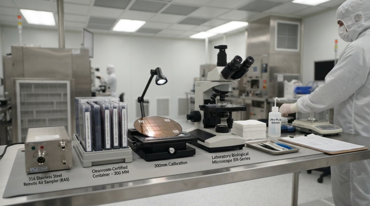
Prepare calibration equipment by powering on instruments at least 30 minutes before use for thermal stabilization. Verify light sources function and optics are clean. Run system diagnostics and confirm all sensors respond correctly. Document ambient conditions, temperature, humidity, and atmospheric pressure affect measurement accuracy.
Phase 2: Wafer Inspection and Defect Detection Setup
Mount the calibration wafer on your inspection system according to manufacturer instructions. Ensure the wafer is positioned flat and centered. Configure the inspection system for the specific wafer, selecting appropriate detection thresholds for particle sizes present. Run a system self-check to verify laser power, detector sensitivity, and signal processing. Address any warnings before proceeding.
Phase 3: Measurement Execution and Error Correction
Scan the calibration wafer following standard protocol. Capture data from the entire wafer or predetermined regions. Most systems allow multiple scans, providing repeatability data revealing whether equipment is stable or drifting.
Record raw measurement results and compare to certified values. Calculate count efficiency: (particles detected / particles certified) × 100. Apply the 16-term error model correction if your system supports it, though error correction cannot fix fundamental equipment problems.
Measure uniformity across the wafer. Particle detection often varies by location. Document variations; if they exceed acceptance criteria (typically ±10%), investigate the cause, uneven illumination, detector sensitivity variations, or stage positioning errors.
Phase 4: Data Validation and Certification
Compare measurement results to certified values. Typical acceptance windows are ±5% for count accuracy and ±3% for particle size measurements. If results fall within acceptance criteria, document the successful calibration with date, time, equipment serial number, operator name, and results. Store documentation according to quality system requirements.
If results fall outside acceptance criteria, do not use that equipment for production measurements. Investigate the cause, optical contamination, detector aging, software drift, or mechanical misalignment. Contact your equipment manufacturer’s service department if you cannot identify the problem.
Establish a calibration schedule. Most operations calibrate critical equipment weekly or monthly depending on stability and measurement criticality. Particle counters might be calibrated monthly; thin film systems weekly.
Common Calibration Failures and Troubleshooting
Particle contamination on the calibration wafer itself is common. If a PSL wafer sits in a cleanroom for months without proper storage, it accumulates unwanted particles. Retire contaminated wafers and use fresh ones. Always store calibration wafers in sealed containers in cleanroom environments.
Wafer uniformity issues emerge when particle deposition wasn’t uniform during manufacturing. Some regions have higher particle density than others. Check whether the certified specification includes uniformity data. If certification states uniform distribution but you measure significant variations, the wafer may be defective.
Measurement uncertainty problems arise when system uncertainty exceeds process tolerance. If a thin film system has ±10 nanometer uncertainty but your process requires ±5 nanometer accuracy, you cannot use that system for process control. Either improve the measurement system’s accuracy or accept wider tolerance.
The 16-term error model assumes systematic errors remain constant. If equipment is drifting, detector sensitivity decreasing, for example, error correction becomes less effective. Measurement results drift progressively away from certified values, signaling that maintenance is needed.
Thin film measurement challenges often involve optical interference effects. Small variations in wavelength, angle of incidence, or refractive index produce large thickness variations. If measurements consistently exceed or fall short of certified values, adjust wavelength calibration or verify film material properties in software.
XRF (X-ray fluorescence) measurement for elemental composition requires reference materials with known composition. If your XRF system drifts, the X-ray tube intensity may be changing due to aging or the detector needs recalibration.
The fastest path to measurement credibility is establishing a disciplined calibration schedule and documenting every result. Most measurement failures trace back to skipped calibrations or inadequate documentation, not equipment defects.
In-House vs. Third-Party Calibration: Cost-Benefit Analysis
In-house calibration requires upfront investment in equipment and training. You’ll need calibration wafers (several hundred dollars per wafer), measurement equipment, and cleanroom space. For organizations with dozens of pieces requiring frequent calibration, this investment can pay dividends. You maintain control over process, documentation, and scheduling.
Hidden costs often exceed direct equipment costs. Calibration downtime, hours your equipment is offline, directly impacts production. For high-volume operations, this cost can be substantial. Validation downtime compounds the problem; after calibration, you may need to validate equipment functionality before returning it to production.
Third-party calibration services handle everything externally. You ship equipment or calibration wafers to a certified provider. They perform calibration, document results, and return everything. The advantage is minimal downtime; the disadvantage is cost per calibration event.
Many organizations use a hybrid approach. Critical equipment gets third-party calibration with NIST traceability. Monitoring equipment or less critical systems get in-house calibration to control costs.
Partner with external services when: your organization lacks cleanroom infrastructure, you have few pieces requiring occasional calibration, regulatory requirements demand third-party documentation, or you lack internal expertise in specific measurement techniques.
Applications of Calibration Wafer Standards in Semiconductor Production
Wafer inspection systems like Surfscan defect detection tools use PSL calibration wafers to verify detection at required sensitivity. Advanced node manufacturing (5nm, 3nm, and beyond) requires detection of particles smaller than 10 nanometers. Calibration wafers with certified sub-10nm particles verify your inspection system achieves this sensitivity.
Process control measurements rely on calibration standards for thin film thickness, dopant concentration, and other critical parameters. These measurements are only meaningful if the measurement system has been calibrated against reference materials with known properties.
Yield analysis often reveals patterns tracing back to measurement errors. A calibration wafer with particles distributed across different regions helps identify whether problems are actual defects or measurement artifacts.
Selecting the Right Calibration Wafer Standard for Your Process
Calibration wafers come in different diameters. Your equipment must accommodate the wafer size, and the wafer must match your manufacturing process.
125mm wafers are legacy sizes, rarely used in modern production but present in some research environments. Applied Physics offers 125mm calibration wafer standards.
200mm wafers dominate specialized applications, compound semiconductors, MEMS, power devices, and some analog/mixed-signal production. Applied Physics provides 200mm calibration wafer standards.
300mm wafers are the industry standard for high-volume logic and memory production. Applied Physics offers 300mm calibration wafer standards designed for these environments.
IEEE standards provide guidance on calibration requirements for semiconductor equipment. The IEEE standards for semiconductor metrology establish best practices for measurement uncertainty, traceability, and documentation.
Selecting the right specification involves matching particle sizes, thin film thicknesses, or other parameters to your process requirements. Work with your equipment manufacturer and calibration service provider to specify the right standard for your specific process.
Conclusion
Semiconductor wafer calibration standards guide your organization toward measurement credibility and regulatory compliance. The investment in proper calibration directly protects product quality and customer confidence.
Applied Physics has supported semiconductor manufacturers since 1992 with precision calibration wafer standards across 125mm, 150mm, 200mm, and 300mm formats. Our NIST-traceable standards come with complete documentation and measurement uncertainty statements. Whether you’re calibrating particle inspection systems, thin film measurement equipment, or RF characterization tools, Applied Physics calibration wafers provide the reference accuracy your measurements demand. Contact Applied Physics today to discuss your specific calibration requirements and ensure your metrology systems remain within specification.
| Calibration Phase | Key Activities | Success Criteria |
|---|---|---|
| Pre-Calibration Preparation | Verify wafer certification, inspect for contamination, prepare environment | Cleanroom verified, equipment warmed up, ambient conditions documented |
| Wafer Inspection Setup | Mount wafer, configure detection thresholds, run diagnostics | Equipment self-check passed, wafer positioned correctly |
| Measurement Execution | Scan wafer, record results, apply error correction | Results within ±5% of certified values, uniformity acceptable |
| Data Validation | Compare to certified values, document results, establish schedule | Documentation complete, acceptance criteria met, schedule established |
Frequently Asked Questions
What are semiconductor wafer calibration standards and why do manufacturers need them?
Semiconductor wafer calibration standards are precision reference wafers used to verify the accuracy and performance of metrology equipment in semiconductor manufacturing. These standards contain known particles, defects, or thin film deposits that allow equipment to be validated against NIST-traceable measurements. Manufacturers need them to ensure their wafer inspection systems, particle counters, and measurement tools deliver accurate results, critical for maintaining yield rates and meeting customer specifications, especially at advanced nodes where sub-10nm particle detection is essential.
Why are NIST traceable wafer standards important for semiconductor manufacturing?
NIST traceability establishes a chain of measurement confidence from your calibration wafer back to national standards. This means your equipment's measurements are scientifically defensible and recognized globally. For semiconductor manufacturers, NIST traceable standards reduce measurement uncertainty, support regulatory compliance, and provide documentation that auditors and customers require. Without NIST traceability, you cannot prove your metrology is accurate, a critical gap for advanced node production and quality audits.
What is the difference between PSL wafer standards and other calibration wafer types?
PSL (polystyrene latex) wafer standards use precisely deposited PSL spheres of known sizes to calibrate particle counting and defect detection equipment. These standards are ideal for validating surfscan and wafer inspection systems because the particles mimic real contamination. Other calibration types include thin film standards for XRF measurement and metallic waveguide standards for RF characterization. PSL standards are most common in semiconductor because they directly validate the particle detection capability your equipment needs for cleanroom contamination control.
How often should semiconductor wafer inspection tools be recalibrated with calibration standards?
Calibration frequency depends on equipment type, usage intensity, and regulatory requirements. Most semiconductor manufacturers recalibrate inspection tools quarterly or semi-annually, though high-volume production environments may calibrate monthly. Equipment experiencing frequent use or supporting critical process nodes should be calibrated more often. Your calibration schedule should be documented and traceable; check your equipment's user manual and your facility's quality procedures for specific intervals. Unexpected measurement drift or failed audits may also trigger unscheduled recalibration.
