
Particle contamination on silicon and film-deposited wafers occurs when unwanted nano- or micro-scale particles settle on wafer surfaces during semiconductor processing. These particles can disrupt lithography, seed defects in deposited films, and reduce yield—especially at advanced process nodes. Effective contamination control depends on accurate inspection, proper tool calibration, and an understanding of how wafer surfaces and film stacks influence particle detectability.
Particle contamination remains one of the most persistent yield and reliability risks in semiconductor manufacturing. Even a single particle can introduce a defect that impacts electrical performance, causes opens/shorts, or creates localized failure mechanisms that appear later in reliability testing.
As device geometries shrink and process windows tighten, fabs must detect smaller particles, control more contamination sources, and interpret inspection data across a wider range of wafer surfaces—including bare silicon and complex film stacks.
Particles can be introduced at multiple points across the manufacturing flow, including:
Once present, particles can migrate and deposit by gravity, electrostatic attraction, thermophoresis, and Brownian motion—especially in high-flow and high-temperature tool environments.
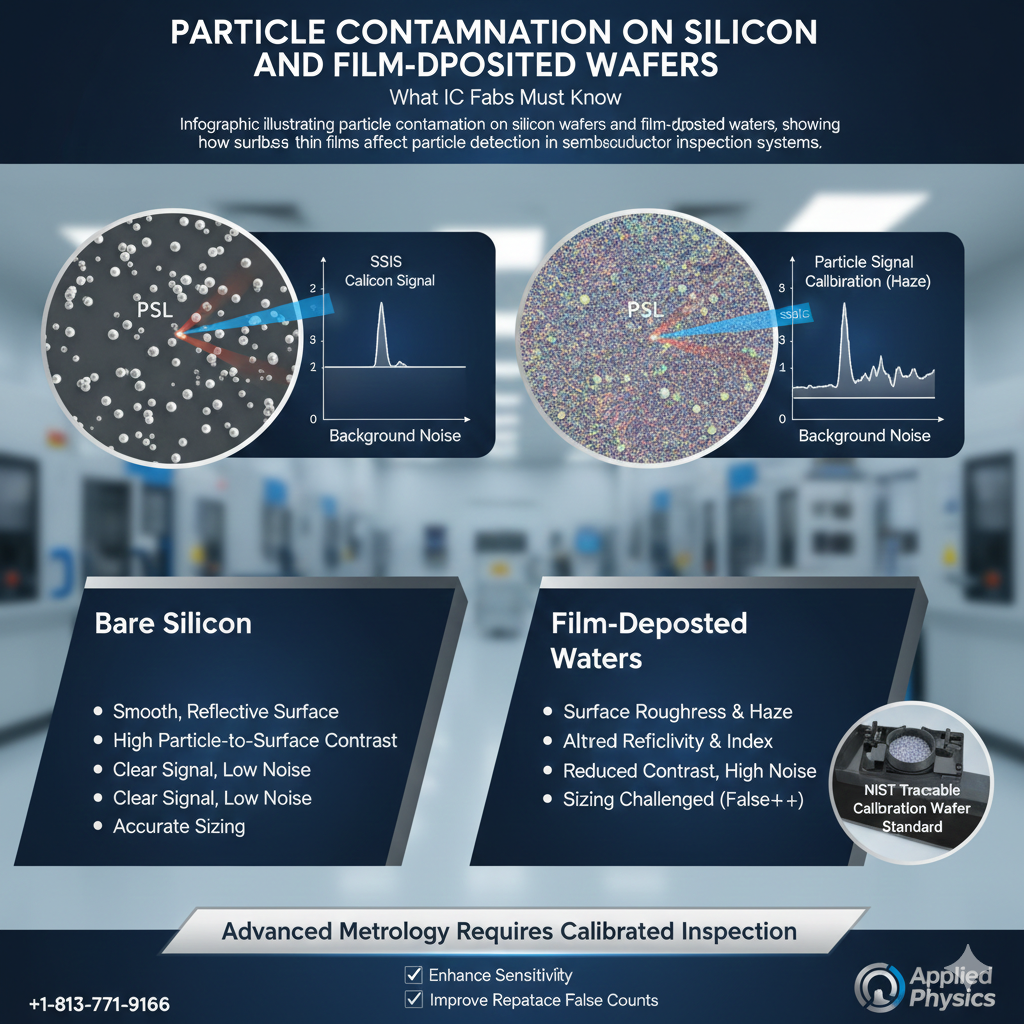
Most wafer surface particle monitoring is performed using laser-based Surface Scanning Inspection Systems (SSIS) and wafer scanners. These systems illuminate the wafer and measure scattered light; particles scatter differently than the underlying surface, producing a signal that can be detected, counted, and (in many systems) converted into an estimated particle “size” based on calibration.
Key variables that influence detection include:
Because particle “size” in optical inspection is a calibrated measurement rather than a direct physical measurement, calibration standards and recipe stability are essential for repeatable metrology.
Film-deposited wafers introduce additional challenges because the surface the inspection system “sees” is no longer a simple silicon reflectance condition.
Film stacks can change particle detectability due to:
As a result, the same physical particle may appear “larger,” “smaller,” or even fall below detection thresholds depending on film material, thickness, and inspection wavelength.
Optical inspection sensitivity is limited by signal-to-noise ratio. Rougher surfaces and certain deposited films can increase background scatter (“noise”), which can cause:
This is one reason advanced fabs routinely tune inspection recipes by wafer type and film stack—and why metrology teams rely on stable calibration and reference wafers to track drift.
Because optical “particle size” is derived from scattering behavior, calibration wafer standards help ensure inspection tools report consistent results over time and across tool fleets.
High-quality calibration programs support:
At Applied Physics Inc. (founded in 1992 in Colorado and now operating in Tampa, Florida), we support semiconductor metrology teams with calibration wafer standards and technical guidance designed to improve repeatability, comparability, and confidence in particle inspection data.
Internal link suggestion (add in editor): Link the phrase “calibration wafer standards” to your Applied Physics calibration wafer product page.
While every fab environment is unique, contamination control programs commonly include:
Particle contamination affects both bare silicon and film-deposited wafers, but film stacks introduce additional optical complexity that can change particle detectability and sizing behavior. For advanced nodes, contamination control requires more than cleanroom classification—it requires inspection systems tuned to surface conditions and verified using stable, traceable calibration standards.
Particle contamination is commonly caused by airborne particles, process tool wear, chamber byproducts, chemical residues, and wafer handling or transport environments. Even in advanced cleanrooms, particles can be introduced during maintenance events, process steps, or within mini-environments like FOUPs.
Films change reflectivity, refractive index, and surface roughness, which can increase background scatter and reduce contrast between particles and the wafer surface. This can shift sensitivity thresholds and make sizing less stable compared to bare silicon.
SSIS tools illuminate the wafer using a laser and measure scattered light. Particles scatter light differently than the wafer surface, producing signals that can be counted and converted into estimated particle sizes using calibration.
At advanced nodes, very small particles can create killer defects depending on where they land and what process step follows. The risk increases as feature sizes shrink and process margins tighten, making sensitive inspection and stable calibration increasingly important.
Optical particle “size” is a calibrated measurement based on scattering behavior, not a direct physical measurement. Calibration ensures particle sizing and counting remain repeatable over time, supports tool matching across fleets, and improves confidence in contamination monitoring data.
Most fabs use NIST-traceable particle calibration wafer standards (often PSL or silica-based, depending on inspection wavelength and tool design) to verify sizing peaks, threshold behavior, and long-term drift.
For technical questions related to contamination monitoring, inspection calibration, or wafer standard selection, contact Applied Physics in Tampa, Florida.
Phone: +1-813-771-9166
Since 1992, Applied Physics Corporation has been a leading global provider of precision contamination control and metrology standards. We specialize in airflow visualization, particle size standards, and cleanroom decontamination solutions for critical environments.