SSIS tools (Surface Scanning Inspection Systems) must be calibrated to NIST-traceable particle size standards to ensure particle sizing is consistent, comparable, and actionable across tools, fabs, and time. When particle size data is accurate and standardized, contamination control teams can identify sources faster, reduce false alarms, improve tool matching, and protect yield—especially at advanced nodes where small particles can become killer defects.
SSIS tools are used worldwide to monitor unwanted particle contamination on production substrates, including:
These systems scan a surface using controlled illumination and measure scattered light captured by a detector. The tool’s software converts that scatter signal into particle “size” based on a calibration curve. In other words: particle size is a calibrated response, not a direct physical measurement.
That is why calibration to known standards matters.
As particle counts rise, wafer yield and throughput fall. Metrology teams then need to answer practical questions quickly:
The only reliable way to compare results across different SSIS tools—and across different manufacturing sites—is to reference particle sizing to a common, traceable diameter standard. NIST traceability creates a shared measurement “language” so contamination data can be interpreted consistently across teams and locations.
In semiconductor contamination control, NIST traceability is anchored to NIST Standard Reference Materials (SRMs) at specific particle diameters commonly used to validate particle sizing response. These SRMs serve as calibration anchors for particle sizing programs and for traceability chains used by labs producing particle size standards.
A key point in high-precision calibration programs is this:
Precision matters at the nanometer scale.
For example, 895 nm is not the same as 1 µm (1000 nm), and treating them as equivalent introduces avoidable calibration error. Accurate calibration depends on using the true reference diameter—not informal rounding—especially when correlating performance across tools and sites.
Particle detection capability is limited by signal-to-noise ratio (S/N). Even on prime wafers, background scatter exists due to real surface roughness at microscopic levels. As surfaces become optically “noisier,” small particles become harder to discriminate from the background.
Film stacks can make detection and sizing significantly more complex because films can change:
This can cause the same physical particle to appear “different” to the inspection system depending on film type and thickness—meaning calibration and recipe alignment must account for real surface conditions.
SSIS detectors receive two dominant components during scanning:
Large particles generate strong AC pulses that are easy to detect. As particles get smaller, the scatter signal drops rapidly, and discrimination becomes challenging—especially when background noise rises due to surface condition or film deposition.
This is why calibration wafers must be stable, well-characterized, and aligned to the tool’s detection regime.
Over time, wafer surfaces can change due to environmental exposure and natural surface chemistry. Even small changes in surface condition can increase background scatter and reduce sensitivity to the smallest particles.
For contamination control programs targeting very small particle regimes, this means:
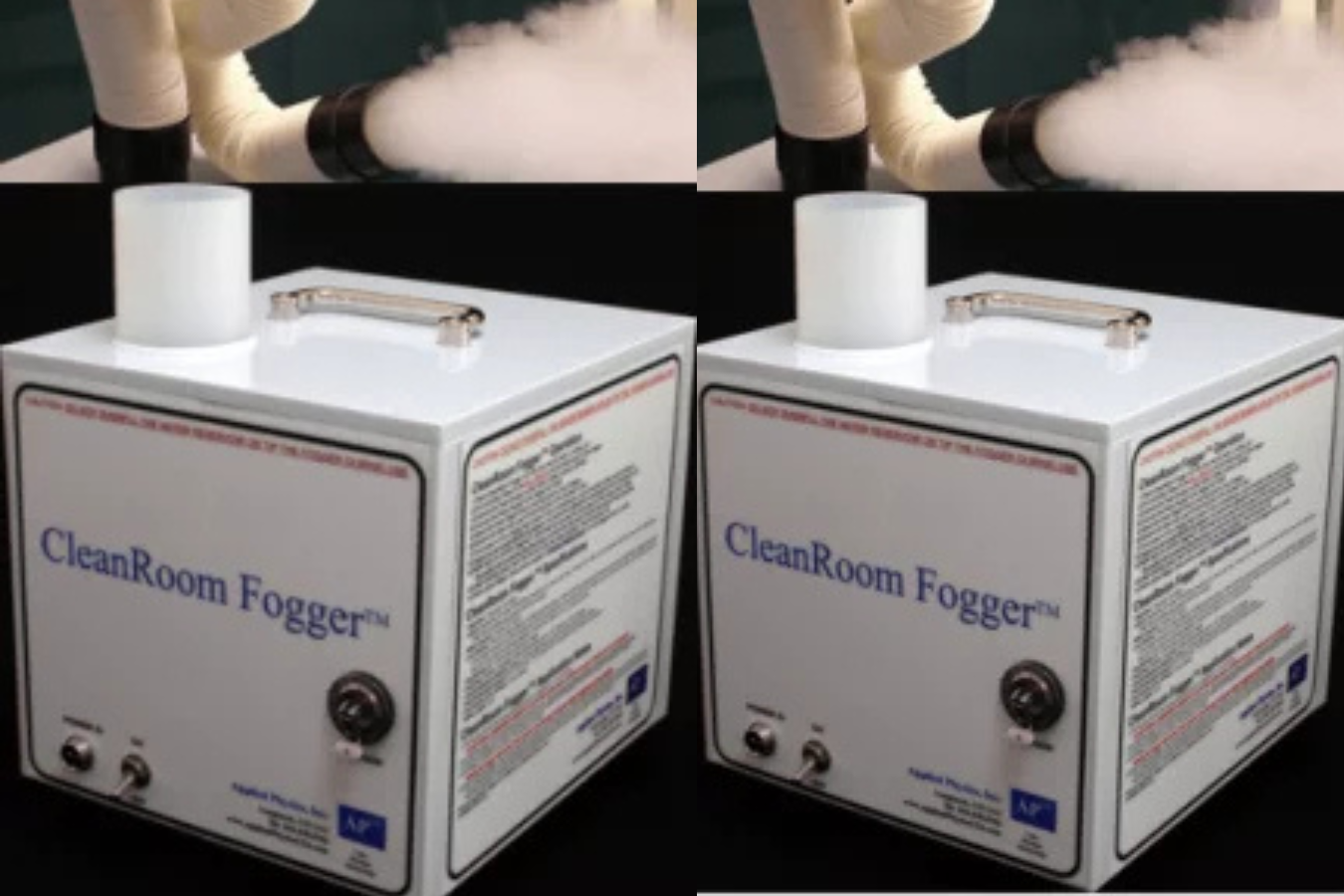
Many metrology teams use calibration wafer standards with:
Multi-peak standards enable verification of sizing response at several diameters in one run and can reveal drift that may not be obvious at a single calibration point.
Even when sizing is tightly aligned, counts can vary between tools due to differences in:
Modern fleets often manage this with procedural controls (and, where applicable, software normalization) while keeping sizing traceability anchored to known standards.
At Applied Physics Inc. (founded in 1992 in Colorado, now operating from Tampa, Florida), we support contamination control and metrology teams with:
The practical goal is simple: use a shared, NIST-traceable sizing reference so contamination data leads to faster root-cause decisions and higher manufacturing efficiency.
For SSIS calibration questions, wafer standard selection, or technical review of your inspection regime:
Phone: +1-813-771-9166
An SSIS tool scans wafer, mask, or film surfaces to detect and size unwanted particles using optical scatter signals. It is a primary metrology tool for contamination monitoring and process control in semiconductor manufacturing.
NIST traceability provides a common diameter reference so particle sizing data is comparable across different tools, fabs, and time. This improves tool matching, reduces misinterpretation, and helps teams locate contamination sources faster.
Sizing is anchored to calibration response curves, while counts can vary due to laser power, beam geometry, optics, and tool aging. Many fleets manage this with procedural controls while keeping sizing traceability consistent.
Film stacks change optical properties and can increase background scatter or interference effects. This reduces signal-to-noise for small particles and can alter apparent sizing response unless calibration and recipes account for the surface condition.
Verification frequency depends on tool stability, contamination risk, and process criticality. Many teams verify on a routine schedule and after maintenance, process changes, or evidence of drift in contamination data.
Not always. Precision matters. For calibration programs, reference diameters should be treated as their true values, not rounded labels, especially when correlating performance across multiple sites and tools.