The semiconductor industry’s march toward the angstrom era has fundamentally altered the physics of manufacturing.
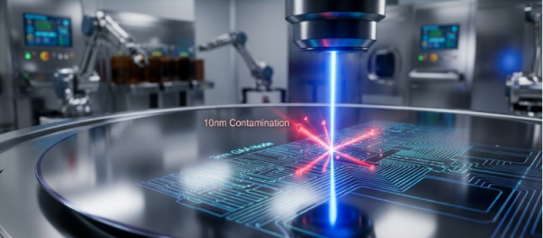
As fabs transition to 5nm, 3nm, and 2nm nodes, the margin for error has effectively vanished. In this regime, a defect the size of a single DNA strand can render a chip useless.
For yield engineers, the challenge is no longer just finding defects; it is distinguishing signal from noise in an environment where the features themselves are barely larger than the wavelengths of light used to measure them.
This article explores the advanced metrology technologies, specifically the convergence of optical, e-beam, and AI, that are making sub-10nm defect classification possible.
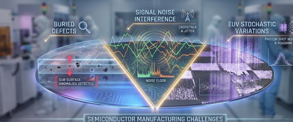
To understand the solution, we must first appreciate the problem. Manufacturing at the sub-10nm node introduces three critical hurdles.
In planar 2D transistors, defects were largely surface-level.
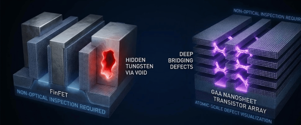
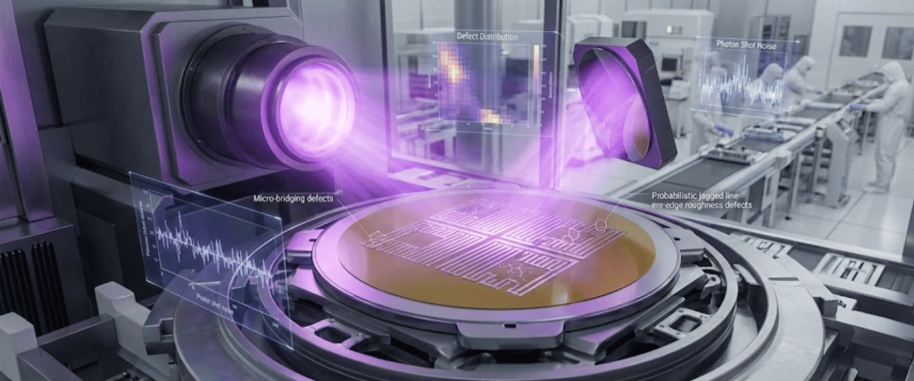
In modern 3D architectures like FinFETs and GAA nanosheets, defects are often buried. A void inside a tungsten via or a bridge deep between fins is invisible to standard optical tools.
As feature sizes shrink, the scattering signal from a defect weakens.
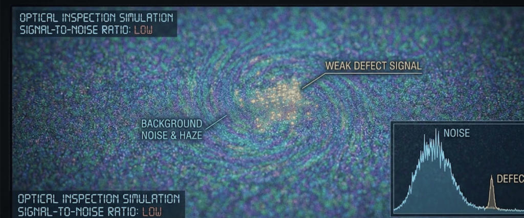
Simultaneously, surface roughness (haze) and process variations create noise. Traditional threshold-based detection struggles here, often flagging thousands of nuisance events (false positives) that drown out the real defects.
The adoption of Extreme Ultraviolet (EUV) lithography has introduced stochastic (random) defects such as line-edge roughness and micro-bridging that are probabilistic in nature.
Catching these requires inspecting vast areas of the wafer, which challenges the throughput of high-resolution tools.
The industry has responded with a Hybrid Metrology approach, blending the speed of light with the precision of electrons.
BBP systems remain the workhorse for high-volume manufacturing.
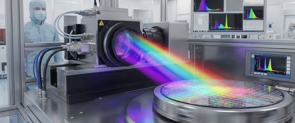
By utilizing a super-continuum light source (ranging from DUV to visible), these tools can be tuned to specific wavelengths that resonate with the materials on the wafer.
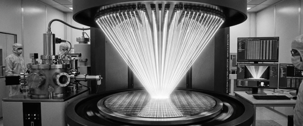
E-beam inspection offers the ultimate resolution (sub-1nm) but has historically been too slow for inline monitoring. The breakthrough lies in Multi-Beam technology.
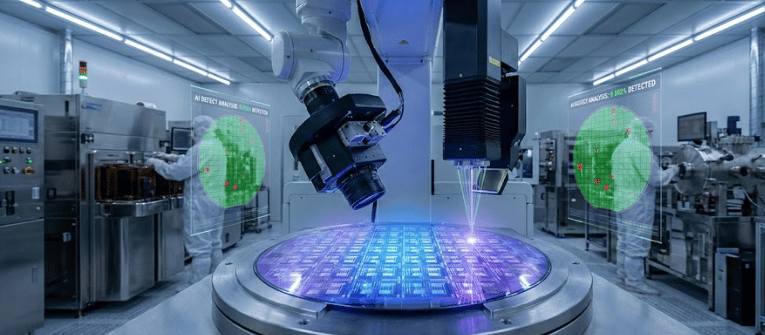
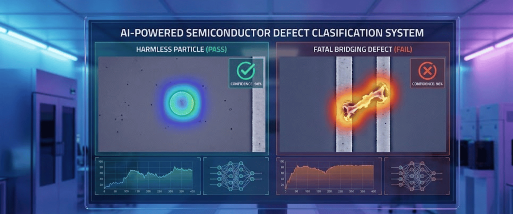
Hardware allows us to see the defect; software allows us to understand it. The sheer volume of data generated by multi-beam and BBP tools renders manual classification impossible. This is where Deep Learning enters the fab.
Legacy ADC relied on rule-based algorithms (e.g., if blob is round, it is a particle). These rules break down at 5nm.
Training an AI requires massive datasets of defects, which are rare in a mature process.
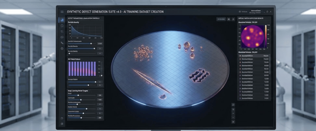
Advanced metrology providers are now using synthetic data generation, creating realistic simulations of defects to train their models before the first wafer is even processed.
As we look toward the High-NA EUV era and 3D stacking (Chiplets), metrology will move from Post-Process to In-Situ.
The survival of Moore’s Law depends as much on metrology as it does on lithography.
By leveraging the synergy of Broadband Plasma, Multi-Beam E-Beam, and Deep Learning, semiconductor manufacturers can illuminate the sub-10nm landscape, transforming raw data into the high yields required for the AI and high-performance computing revolution.
At the sub-10nm level, defects are often smaller than the wavelength of light used by standard tools. This creates a low signal-to-noise ratio, making it extremely hard to distinguish a killer defect from harmless surface roughness or background noise.
Optical inspection (Broadband Plasma) is fast and best for scanning entire wafers. E-Beam inspection offers much higher resolution (sub-1nm) to see the tiniest details, but it is naturally slower. Modern Multi-Beam systems bridge this gap by using thousands of beams at once to increase speed.
AI uses Deep Learning to automatically analyze thousands of images in real-time. It can instantly tell the difference between a fatal bridge or a short and a harmless particle, allowing engineers to fix production issues much faster without manual review.