In modern semiconductor manufacturing, optical inspection tools are only as reliable as the standards used to calibrate them. As critical dimension control tightens and defect budgets shrink, selecting the right calibration wafer standard is no longer a formality—it is a foundational requirement for process control, tool matching, and regulatory confidence.
At Applied Physics., we work directly with semiconductor fabs, advanced packaging facilities, and inspection tool owners to design NIST-traceable calibration wafer standards that align with real-world process conditions. Below is a practical framework for choosing the optimal calibration wafer for optical inspection systems.
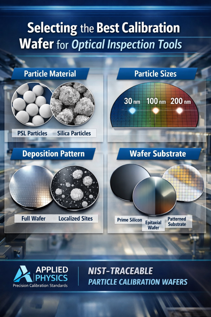
The first—and most critical—decision is particle material, as it directly impacts optical response and measurement repeatability.
PSL (Polystyrene Latex) microspheres remain the industry standard for optical inspection calibration. Their advantages include:
These characteristics make PSL ideal for calibrating surface inspection tools used to detect particles, haze, and pattern defects.
In applications requiring higher thermal stability, chemical resistance, or mechanical durability, silica particle calibration wafers may be preferred. While silica is less optically efficient than PSL, it offers robustness for specific process environments or long-term reference use.
Best practice: Use PSL for optical sensitivity calibration and silica where environmental durability is the primary concern.
Particle size selection should directly align with the detection thresholds and recipes used on the inspection tool—not arbitrary nominal values.
Effective calibration strategies often include:
At Applied Physics, all particle sizes are NIST-traceable, ensuring measurements are repeatable, auditable, and comparable across tools, fabs, and time.
Deposition pattern plays a major role in how accurately calibration wafers simulate production conditions.
Common approaches include:
Configurable deposition patterns allow engineers to stress the inspection system where it matters most—rather than relying on overly uniform or unrealistic test conditions.
Calibration wafers are most effective when the substrate closely matches production wafers.
Substrate options commonly include:
Matching reflectivity, surface roughness, and film stacks ensures that optical response during calibration mirrors actual process behavior—reducing false confidence and improving tool-to-tool matching.
For fabs operating under ISO, USP, or customer audit requirements, documentation matters.
High-quality calibration wafer programs often include:
These artifacts support long-term monitoring, cross-fab comparability, and defensible metrology practices.
What calibration wafers are used for optical inspection tools?
Calibration wafers used for optical inspection tools typically contain NIST-traceable PSL or silica particles deposited on silicon wafers. These wafers are used to verify tool sensitivity, particle detection thresholds, and inspection recipe accuracy in semiconductor manufacturing.
Why are PSL particles preferred for optical inspection calibration?
PSL particles are preferred because they provide uniform size, spherical shape, and predictable light scattering. This makes them ideal for calibrating bright-field and dark-field optical inspection systems where measurement repeatability is critical.
How do I choose the right particle size for calibration wafers?
The correct particle size should match the minimum detectable size and inspection recipe of the tool. Many fabs use multiple particle sizes on a single wafer to validate sensitivity roll-off and ensure accurate threshold detection.
What is the difference between full-wafer and localized deposition?
Full-wafer deposition is used for baseline qualification and benchmarking, while localized deposition simulates real defect distributions and supports recipe tuning without introducing unnecessary background noise.
Why does wafer substrate matter for optical inspection calibration?
Wafer substrate impacts reflectivity and optical response. Calibration wafers should closely match production substrates—such as prime silicon, epitaxial wafers, or patterned surfaces—to ensure realistic tool response.
Are calibration wafers required to be NIST-traceable?
While not always mandatory, NIST traceability ensures measurements are repeatable, auditable, and comparable across tools, fabs, and time—making it a best practice for advanced semiconductor manufacturing.
The “best” calibration wafer standard is not a catalog item—it is a process-matched reference that balances realism, traceability, and repeatability.
Applied Physics specializes in configurable optical inspection calibration wafers designed to:
Our standards are used globally by semiconductor manufacturers, equipment owners, and metrology teams who require confidence—not assumptions—in their inspection data.
(KLA)
Calibration wafers for KLA optical inspection tools must support tight sensitivity thresholds, stable light-scattering behavior, and repeatable defect detection across tool fleets.
PSL particle calibration wafers are commonly used to verify bright-field and dark-field sensitivity, tool matching, and recipe stability across multiple KLA platforms.
(Applied Materials)
Optical inspection calibration for AMAT platforms requires wafer standards that match production substrates and process conditions.
Configurable particle sizes, substrate options, and deposition patterns enable accurate calibration during tool qualification, process development, and ongoing monitoring.
(Hitachi High-Tech)
Hitachi optical inspection systems benefit from calibration wafers with highly uniform particle geometry and predictable optical contrast.
Multi-size PSL particle wafers are commonly used to validate detection sensitivity and ensure consistent performance across inspection modes.
Fabs operating mixed inspection fleets require standardized, NIST-traceable calibration wafers to ensure cross-platform comparability.
Using consistent particle materials, sizes, and substrates enables reliable tool matching and reduces measurement drift across OEMs.
Since 1992, Applied Physics Corporation has been a leading global provider of precision contamination control and metrology standards. We specialize in airflow visualization, particle size standards, and cleanroom decontamination solutions for critical environments.