Last Updated: August 16, 2026
Particle contamination is the silent yield killer in semiconductor fabrication. A single sub-micron particle landing on a wafer during photolithography can render the entire die unusable. This operational reality separates fabs running at 95% yield from those struggling at 75%. Particle counting for semiconductor fabrication has become non-negotiable for any operation targeting advanced nodes, where precision requirements increase exponentially as process geometries shrink below 10 nanometers.
Each percentage point of yield loss translates directly to millions in lost revenue. A 300mm wafer fab producing 10-nanometer devices loses roughly $50,000 in potential revenue per percentage point of yield degradation. Applied Physics has spent over three decades helping fabs quantify and control contamination.
Particle counting is about understanding your contamination profile: measuring particle size distribution, identifying elemental composition, and tracking temporal trends to attack root causes rather than treating symptoms.
Real-time particle monitoring transforms contamination control from reactive troubleshooting into predictive management. Instead of discovering yield problems weeks after they occur, you detect contamination events as they happen and respond within hours.
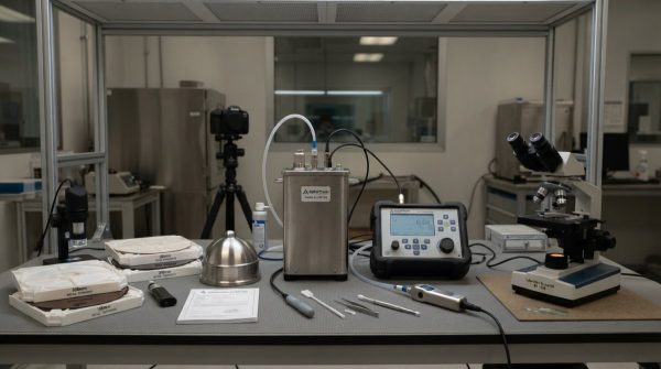
Optical particle counters positioned strategically throughout your fab measure particle concentration in real time, detecting particles as small as 0.3 micrometers and capturing size distribution data that reveals whether contamination originates from ambient air infiltration, tool outgassing, or chemical degradation. When a sensor detects an anomalous particle event, your team can immediately investigate the source before those particles reach your wafer.
Cleanrooms operating at ISO 14644 Class 5 standards maintain particle concentrations below 3,520 particles per cubic meter at 0.5 micrometers and larger. Exceeding that threshold causes defect density to climb measurably. Real-time monitoring lets you track whether your cleanroom is drifting toward that limit, providing advance warning to increase air changes, tighten access controls, or schedule maintenance.
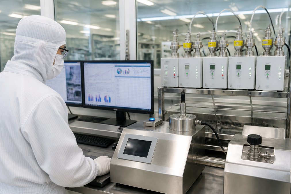
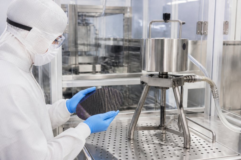
Applied Physics calibration wafer standards provide the reference needed to validate your particle counting equipment itself. Without proper calibration, your particle counter becomes a source of uncertainty rather than confidence. The most effective fabs treat their metrology equipment with the same rigor they apply to their process tools.
Continuous monitoring reveals temporal patterns that static sampling misses. You might discover that particle concentration spikes when a particular tool runs a specific recipe, or climbs during personnel shift changes. These insights drive targeted interventions, equipment maintenance, process recipe adjustments, or cleanroom protocol refinements, that wouldn’t emerge from quarterly sampling.
ISO 14644 defines the classification system governing cleanroom particle monitoring standards worldwide. Class 5 cleanrooms (the typical requirement for semiconductor fabrication at advanced nodes) must maintain fewer than 3,520 particles per cubic meter at 0.5 micrometers or larger.
Compliance verification requires documented sampling at defined locations and frequencies, typically at the point of use directly above wafer processing areas where contamination risk is highest. Isokinetic probe design, flow rate control, and sensor placement all influence whether your measurements reflect actual exposure or produce false negatives.
A common mistake is assuming one particle counter in the corner of your cleanroom provides adequate coverage. You need spatial distribution across multiple measurement points to capture the variation in particle concentration that inevitably exists in any real cleanroom.
The regulatory pressure is real. FDA guidance for pharmaceutical manufacturing and semiconductor fabs serving defense or aerospace markets face similar scrutiny. Cleanrooms that maintain documented ISO 14644 compliance attract higher-value customers and command premium pricing for their capacity.
Applied Physics provides solutions to support cleanroom particle monitoring standards programs.
Sub-micron particles are the threat that keeps process engineers awake. Particles smaller than 0.5 micrometers can penetrate defect-prone areas on advanced nodes where conventional contamination control strategies fail. Aerosol particle detection requires different instrumentation than larger-particle monitoring.
Optical particle counters excel at detecting particles down to 0.3 micrometers, but below that threshold, specialized equipment is needed. Condensation particle counters can detect particles as small as 0.01 micrometers by growing them to optically detectable size. For semiconductor fabs, the practical sweet spot is 0.1 to 0.5 micrometers, where aerosols pose the greatest risk to sub-10nm processes.
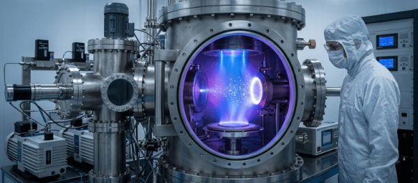
Sub-micron contamination sources are often harder to pinpoint than larger particles. Aerosol particles can originate from chemical reactions in your gas delivery system, outgassing from materials inside your process chamber, or molecular clustering from your vacuum pump exhaust. Proactive aerosol particle detection lets you identify the source and implement corrective action before wafers reach production.
The control strategy for sub-micron contamination differs from conventional particle control. Larger particles are stopped by mechanical filtration and electrostatic precipitation. Sub-micron aerosols require increased air change rates, higher HEPA filter efficiency, chemical scrubbing of process gases, and sometimes active aerosol suppression during high-risk process steps.
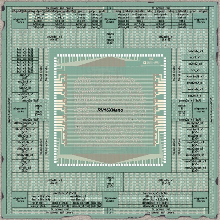
Wafer surface inspection tools represent the final verification layer in your contamination control strategy. While particle monitoring tells you about the environment and process tool cleanliness, surface inspection tools measure the actual outcome, defects on the wafer itself.
Modern inspection systems use optical and electron-beam techniques to detect defects down to the nanometer scale. Optical systems identify particles and material defects on the wafer surface; e-beam tools provide higher resolution for sub-20nm defect detection. The choice depends on your process node and defect sensitivity requirements.
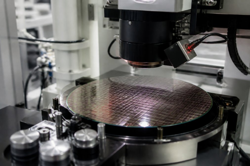
The relationship between wafer surface inspection tools and particle counting is symbiotic. Particle counting reveals what contamination is present in your environment; surface inspection reveals whether that contamination actually reached your wafers and caused defects. Together, they create a closed-loop feedback system. If your particle counts are clean but surface inspection reveals defects, the problem isn’t airborne contamination.
By analyzing defect images from your inspection tools, you can often infer the contamination source and target your control efforts accordingly. The highest-performing operations use inspection data to drive continuous improvement in their contamination control strategy, correlating defect locations with particle count data from specific cleanroom zones.
Semiconductor contamination control best practices form a hierarchy. At the foundation is cleanroom design and maintenance, HVAC systems, filtration, material selection, and access control. The next layer is process tool cleanliness, regular preventive maintenance, chamber conditioning, and gas delivery system monitoring. The top layer is real-time particle counting and process monitoring that catches problems before they reach your wafers.
Most fabs focus heavily on the foundation and neglect the top layer. They maintain their cleanrooms meticulously and service their tools on schedule, but lack visibility into whether those efforts actually prevent contamination. Particle counting closes this gap.
Best practices also include material qualification and supply chain management. Many facilities discover too late that a new chemical vendor’s product has higher particle content than the previous supplier. Incoming material inspection prevents this class of contamination entirely.
Personnel behavior is another critical control point. Even in a well-maintained cleanroom, improper gowning, unnecessary movements, and careless material handling introduce contamination. The best fabs combine cleanroom particle monitoring standards with rigorous personnel training and measure the impact of their gowning protocols by tracking particle concentration before and after personnel entry.
Applied Physics supports contamination control best practices through calibration wafer standards that help validate your measurement systems. If your particle counters are drifting or your optical inspection tools are losing sensitivity, you won’t catch contamination problems until they appear in your yield data.
Particle counting equipment must be integrated into your process tools and cleanroom infrastructure in ways that capture meaningful data without disrupting production. Sensor placement strategy determines whether you get visibility into actual contamination exposure or just measure background noise.
The most critical measurement points are at the point of use, directly above or inside your process chambers where wafers are exposed. Secondary measurement points track ambient cleanroom conditions and gas delivery system cleanliness. Tertiary points might monitor tool exhaust, chemical storage zones, or personnel entry points.
Process tool integration requires careful planning. Sensors must be positioned to capture aerosol and particle streams without interfering with process flow. Sampling lines must be designed for isokinetic flow to avoid particle loss or over-sampling bias. Temperature and humidity control around sampling points matters, as condensation can bias your measurements.
Many fabs over-integrate sensors into their process tools, creating complexity that makes maintenance difficult. The most effective approach is strategic placement, fewer sensors in carefully chosen locations, with rigorous maintenance protocols and regular calibration.
Real-time monitoring doesn’t mean collecting data every second. Most fabs collect particle count data every 1-5 minutes, providing sufficient temporal resolution to detect process-related contamination spikes. During high-risk process steps, you might increase sampling frequency to capture transient contamination events.
Applied Physics calibration wafer standards validate that your integrated sensors are performing correctly. Periodic testing ensures your sensors haven’t drifted and are still providing accurate measurements.
Calibration is where many fabs stumble. Particle counting equipment requires regular calibration against traceable standards. Without it, your particle counter becomes unreliable, potentially reporting clean conditions while contamination is rising.
Drift management means establishing a calibration schedule and following it. Most optical particle counters should be calibrated annually at minimum, more frequently if heavily used. Applied Physics calibration wafer standards provide the reference needed for this validation. Many fabs now perform periodic in-house calibration checks using calibration wafer standards rather than relying on external services that require equipment downtime.
Predictive maintenance uses particle count data to anticipate equipment failures before they occur. If your HEPA filters are degrading, particle concentration will climb gradually before the filter fails completely. If a process tool’s chamber is developing a leak, you’ll see particle concentration spikes during that tool’s operation. By monitoring these trends, you can schedule maintenance proactively rather than reactively.
The data infrastructure for predictive maintenance requires continuous collection, reliable storage, and trend analysis. Many fabs use time-series databases and statistical process control (SPC) charts to visualize particle trends and identify anomalies. When a sensor detects a statistically significant shift in particle concentration, your team investigates the root cause and takes corrective action.
AI-driven predictive maintenance is emerging as a capability that separates leading fabs from the rest. Machine learning models trained on historical particle count data can predict equipment failures weeks in advance, allowing you to schedule maintenance during planned downtime rather than during production runs.
Selecting the right particle counting for semiconductor fabrication requires matching your specific needs to available solutions. Start with your contamination control objectives. Are you primarily concerned with compliance documentation, or do you want real-time process optimization capability?
Next, consider your technical requirements. What particle size range matters most for your process? If you’re manufacturing at 10 nanometers or below, sub-0.5-micrometer detection becomes critical. What’s your required temporal resolution? What’s your spatial coverage?
Applied Physics calibration wafer standards are available in 125mm, 150mm, 200mm, and 300mm formats, allowing you to validate particle counting equipment across your entire fab footprint. Budget considerations are real, but they shouldn’t drive you toward inadequate solutions. An underfunded particle counting program that produces unreliable data costs more in the long run than a properly resourced program that delivers confidence.
Integration with your fab’s IT infrastructure matters more than many operations realize. Modern particle counting systems should integrate with your manufacturing execution system (MES) and provide real-time dashboards. If your particle counter produces data that sits in a separate database, disconnected from your other process information, you’ll struggle to drive actionable insights.
Applied Physics provides solutions for particle counting for semiconductor fabrication as a core process control capability. The fabs that invest in this see measurable improvements in yield, reduced troubleshooting time, and greater confidence in their contamination control strategy.
Particle contamination remains the dominant source of yield loss at advanced nodes. Implementing a comprehensive particle counting program, combining real-time monitoring, cleanroom standards compliance, and calibration discipline, is how leading fabs maintain competitive yields. Applied Physics provides the calibration wafer standards and technical expertise needed to build confidence in your measurement systems. Contact us to discuss how particle counting for semiconductor fabrication can improve your fab’s contamination control strategy and protect your wafer yield.
| Measurement Point | Typical Frequency | Key Metric | Control Action |
|---|---|---|---|
| Ambient cleanroom | Every 5 minutes | Particle concentration (0.5µm+) | Increase air changes if trending high |
| Process tool inlet | Every 1 minute | Aerosol concentration | Investigate chemical system if spike detected |
| Wafer surface | Post-process | Defect density | Correlate with particle count data |
| Calibration check | Monthly | Particle counter accuracy drift | Re-calibrate if drift exceeds 10% |
Particle contamination directly reduces wafer yield and increases defect density. Even sub-micron particles can cause photolithography failures, electrical shorts, and yield loss during semiconductor fabrication. Real-time particle counting detects contamination sources before they affect production, enabling process engineers to maintain yield targets and reduce costly rework. Continuous monitoring also supports compliance with ISO 14644 cleanroom standards and regulatory audits.
ISO 14644-1 defines cleanroom classifications based on particle size distribution and airborne particle concentrations. For semiconductor fabrication, Class 5 cleanrooms allow no more than 3,520 particles per cubic foot larger than 0.5 micrometers. Sub-micron particle detection is critical because particles smaller than 1 micrometer cause the most process damage. Optical particle counters and aerosol detectors measure compliance by monitoring size distribution across multiple particle size ranges in real time.
Particles interfere with photolithography, etch processes, and thin-film deposition, creating defects that render wafers unusable. A single particle landing on a substrate during critical process steps can cause yield loss of 5-15% per batch, depending on node size and process complexity. Chemical contamination and elemental composition of particles determine failure modes. Predictive maintenance using AI-driven particle event analysis helps process engineers identify contamination sources before widespread yield loss occurs, protecting substrate quality and production schedules.
Primary sources include ambient air infiltration through HVAC systems, vacuum system outgassing, process tool emissions during photolithography and etching, personnel shedding skin cells and fibers, and chemical reactions creating secondary particles. Gas purity issues in supply lines and flow rate inconsistencies can generate particles. Continuous monitoring detects these sources by tracking particle event frequency and size distribution patterns. Contamination control strategies address each source: HEPA filtration, process tool maintenance, personnel training, and chemical management protocols reduce particle generation and improve overall cleanroom environment quality.
[EXTERNAL_LINK: ISO 14644 Cleanroom Classification Standards | iso.org]
[EXTERNAL_LINK: FDA Guidance for Aseptic Processing in Pharmaceutical Manufacturing | fda.gov]
[EXTERNAL_LINK: SEMI Standards for Semiconductor Equipment and Materials | semi.org]
[EXTERNAL_LINK: Semiconductor Industry Association Manufacturing Roadmap | sia.org]
[EXTERNAL_LINK: Journal of Semiconductor Technology and Science – Contamination Control Research | jsts.org]
This article was written using GrandRanker

Enter your details below to save your shopping cart for later. And, who knows, maybe we will even send you a sweet discount code :)
Allow notifications to get real-time updates about your shopping cart and who knows, you may even receive a sweet discount code 😊