
Table of Contents
- Traditional Inspection Methods vs. AI-Driven Approaches
- How AI Improves Defect Detection Accuracy in Wafer Inspection
- Machine Learning for Wafer Defect Classification
- Reducing False Alarm Rates in Chip Inspection Systems
- Generative AI and Automated Defect Classification Workflows
- Data-Driven Quality Control and Yield Optimization
- Semiconductor Yield Management Software Integration
- Human-in-the-Loop Workflows and Regulatory Compliance
- Conclusion
- Supporting References
- Frequently Asked Questions
Last Updated: September 3, 2026
Traditional Inspection Methods vs. AI-Driven Approaches
Visual inspection and basic automated systems have been the foundation of semiconductor quality control for decades. Operators examine wafers under microscopes, looking for particles, cracks, and pattern defects. These methods catch obvious flaws but rely heavily on human judgment, fatigue, and training consistency. The process is slow, inspecting a single wafer can take minutes, and defects smaller than the human eye can resolve are easily missed.
AI-driven approaches change this fundamentally. Machine learning algorithms analyze images in seconds, detecting anomalies that would escape human observation. Deep learning models trained on thousands of wafer images learn to recognize defect patterns across multiple layers and process parameters. The speed advantage is immediate: where manual inspection takes minutes per wafer, AI systems process dozens per hour. More importantly, AI doesn’t get tired. It applies the same detection criteria to the first wafer and the ten-thousandth wafer with identical precision.
The real difference isn’t just speed, it’s consistency and scale. Traditional methods plateau at human capability limits. AI systems improve as they encounter more data. A fab running millions of wafers annually generates enough defect data to continuously refine detection models. This creates a feedback loop: more data improves accuracy, which catches more nuanced defects, which feeds back into the model.
Traditional inspection still has a role. It’s valuable for root cause analysis and for training the AI systems themselves. But as the primary quality control mechanism, it’s becoming obsolete. The question isn’t whether AI improves semiconductor defect detection, it’s how quickly fabs can transition their workflows to use it.
How AI Improves Defect Detection Accuracy in Wafer Inspection
AI improves defect detection accuracy through pattern recognition that exceeds human capability. Deep learning models identify defects by analyzing pixel-level image data, detecting subtle variations in intensity, texture, and spatial relationships that indicate manufacturing anomalies. A model trained on labeled defect images learns to distinguish between yield-killing defects, those that render a chip nonfunctional, and nuisance defects that don’t affect performance.
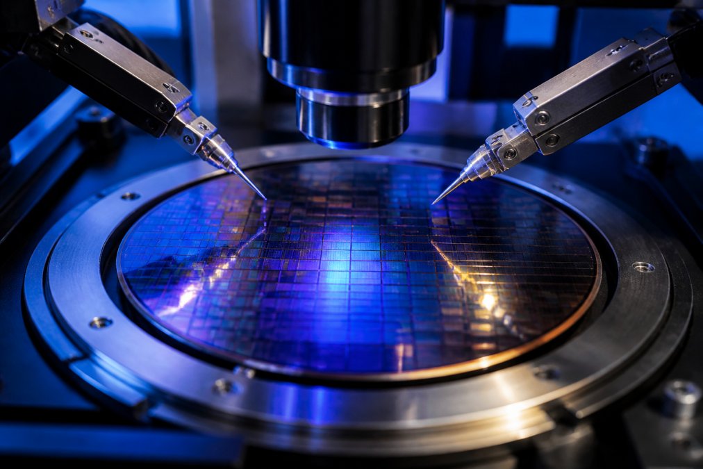
The accuracy improvement comes from scale and consistency. AI systems routinely exceed 95% detection rates for trained defect classes. More significantly, AI maintains that accuracy across shift changes, equipment variations, and process parameter drift. A human inspector’s performance degrades over an 8-hour shift; an AI model’s performance remains constant.
Generative AI adds another dimension. Foundation models trained on diverse manufacturing data can identify defect types the system hasn’t explicitly encountered before. If a new failure mode emerges from a process change, the model can recognize it as anomalous and flag it for human review. This adaptive capability makes AI systems strong to the continuous evolution of fabrication processes.
The integration with design data amplifies accuracy further. When inspection recipes incorporate information about expected pattern geometry, layer stack structure, and design-based inspection rules, the AI system understands what should be present at each process step. It can distinguish between a legitimate design feature and a manufacturing defect that mimics one. This context-aware detection is impossible with traditional methods.
Machine Learning for Wafer Defect Classification
Machine learning algorithms classify defects by learning from historical data rather than following hand-coded rules. During training, the model processes thousands of labeled defect images, learning the visual characteristics that distinguish one defect type from another. A scratch, a particle, a resist residue, and an etch anomaly each have distinct signatures. The model learns these signatures and applies them to new wafers it has never seen.
Automated defect classification (ADC) workflows embed this capability directly into the inspection process. As the inspection tool scans a wafer, it captures images and sends them to the classification model. The model assigns a defect type and confidence score in real time. This immediate categorization allows fabs to make rapid decisions: route this wafer for rework, scrap it, or continue processing based on the defect severity and type.
The accuracy of classification depends on training data quality and quantity. A model trained on 100 defect images will misclassify many real-world defects. A model trained on 10,000 images with diverse process variations, equipment conditions, and failure modes becomes highly reliable. Most semiconductor companies now maintain proprietary defect image databases representing years of accumulated fab data.
Transfer learning accelerates this process. A model pre-trained on a large, diverse defect dataset requires far fewer company-specific examples to achieve high accuracy. Instead of collecting 10,000 images, a fab can fine-tune a pre-trained model with 500 images specific to their process and achieve comparable performance. This is particularly valuable for fabs implementing new nodes or processes where historical data is limited.
Reducing False Alarm Rates in Chip Inspection Systems
False alarms, flagging defects that don’t actually exist or aren’t yield-relevant, waste resources and create bottlenecks. A traditional inspection system with high false positive rates forces operators to manually review thousands of images daily, diluting focus on genuine defects. This is where semiconductor yield management software becomes critical, but the infrastructure choice, where inference happens, directly determines whether false alarm reduction is practical.
AI systems reduce false alarms through confidence scoring and contextual filtering. When the model detects an anomaly, it assigns a confidence score reflecting how certain it is about the classification. The system can be configured to only alert operators for detections above a specific confidence threshold. This threshold is tuned based on the fab’s risk tolerance: conservative settings catch more defects but generate more false alarms; aggressive settings reduce false alarms but risk missing some defects.
Context filtering further reduces nuisance alerts. The system learns which defect types are actually yield-killing and which are cosmetic or self-healing. A small particle on a metal layer might be critical; the same particle on an oxide layer might be irrelevant. By incorporating process knowledge into the classification logic, the system avoids flagging defects that don’t impact yield.
Edge vs. Cloud Processing: The Infrastructure Trade-off
The choice between edge computing (inference on the inspection tool itself) and cloud processing (sending images to remote servers) fundamentally shapes false alarm workflows. Modern inspection tools generate 10-50 gigabytes of image data per hour. Sending all raw images to a cloud service introduces latency, typically 2-10 seconds per wafer, that can bottleneck high-throughput fabs processing 300+ wafers per hour. Edge inference eliminates this latency: the model runs on the inspection tool’s local GPU or FPGA, returning confidence scores and classifications in milliseconds.
However, edge deployment has constraints. The inspection tool’s compute hardware is limited; only smaller, optimized models fit. Cloud-based inference can run larger, more accurate foundation models that catch subtler defects, but the latency cost is significant. Most fabs adopt a hybrid approach: edge inference handles routine, high-confidence classifications in real time, while moderate-confidence detections (60-85% confidence) are sent to cloud systems for deeper analysis. This hybrid model reduces false alarms by leveraging cloud model sophistication only when needed, while maintaining the speed required for continuous wafer flow.
The latency requirement also determines whether human-in-the-loop workflows are operationally viable. If a human reviewer must make a decision within 30 seconds to avoid halting the inspection tool, cloud-based review systems are impractical. Edge-based HITL systems, where the model flags borderline cases and a local fab engineer reviews them on-site, are more feasible. This is why leading fabs are investing in edge AI infrastructure: it enables both faster false alarm reduction and practical human oversight.
Human-in-the-loop workflows address the remaining uncertainty. When the model’s confidence is moderate, say, between 60-80%, rather than making an automatic decision, the system routes the image to a human expert for review. This combines machine speed with human judgment. The expert’s decision feeds back into the model, improving its future performance on borderline cases. Over time, as the model learns from these human reviews, the proportion of images requiring human review decreases. In edge-based systems, this feedback loop is immediate; in cloud systems, latency delays learning cycles by hours or days.
Fabs evaluating AI-driven inspection systems should assess their throughput requirements first. High-throughput fabs (>500 wafers/day) typically require edge inference to avoid bottlenecks. Lower-throughput fabs can tolerate cloud latency and benefit from more sophisticated models. The false alarm reduction strategy must match the infrastructure choice.
Generative AI and Automated Defect Classification Workflows
Generative AI introduces a new capability: synthesizing defect images and understanding defect mechanisms at a deeper level. Foundation models trained on vast amounts of manufacturing data can generate realistic images of defects under various process conditions. This synthetic data augments training datasets, particularly valuable for rare defect types where collecting real examples is expensive.
More importantly, generative AI can explain defects. Instead of just classifying a defect as “etch anomaly,” the model can describe the likely root cause: “etch rate variation in trench structure, consistent with resist erosion during overetch.” This diagnostic capability accelerates root cause analysis. Process engineers don’t have to hypothesize about what caused the defect; the AI system provides an informed assessment based on patterns in the training data.
Automated defect classification workflows powered by generative AI also improve process parameter analysis. The system correlates defect patterns with equipment settings, temperature, pressure, and material properties. Over time, it builds a model of how process parameters influence defect formation. This enables predictive maintenance: the system can warn that a specific tool’s parameter drift is likely to increase defects in the next batch, before defects actually appear.
The integration of design-based inspection with generative AI creates even more powerful workflows. The system understands not just what defects look like, but what they should look like based on the chip design. If a pattern is supposed to be 50 nanometers wide, the system can detect when it’s drifting toward 48 or 52 nanometers. This early warning capability prevents yield loss before it occurs.
Data-Driven Quality Control and Yield Optimization
Data-driven quality control replaces intuition with measurement. Instead of assuming that a process is stable, fabs now collect detailed defect data from every wafer, every layer, every tool. This data feeds into analytics systems that identify trends before they become visible in yield loss. inspection report turnaround.
Predictive analytics systems model the relationship between defect density, defect type, and final yield. They learn that certain defect patterns are strongly correlated with specific failure modes. A high density of small particles on the metal layers might correlate with electromigration failures; the same particles on dielectric layers might be benign. By understanding these correlations, fabs can prioritize defect reduction efforts where they have the highest impact on yield.
Yield optimization becomes systematic. Instead of making process changes based on engineering intuition, fabs now run controlled experiments with careful measurement. The system captures defect data before and after each change, quantifying the impact. Process engineers can see exactly which parameter adjustments reduce which defect types. This accelerates learning and prevents costly mistakes.
The feedback loop is continuous. As new process nodes introduce new defect mechanisms, the data collection and analysis systems adapt. The model learns what defects are problematic at 5 nanometers, 3 nanometers, and beyond. This accumulated knowledge becomes a competitive advantage: fabs with mature data analytics systems ramp new nodes faster and achieve higher yields than competitors still relying on manual troubleshooting.
The real value of data-driven quality control isn’t the technology, it’s the discipline. Fabs that commit to collecting, analyzing, and acting on defect data see yield improvements within the first year. The improvement comes not from a single breakthrough but from systematically addressing the top 10-15 defect drivers, one by one.
Semiconductor Yield Management Software Integration
Semiconductor yield management software ties together inspection data, process parameters, and yield outcomes. It provides the infrastructure for semiconductor defect detection systems to communicate with each other and with manufacturing execution systems (MES).
A modern yield management platform ingests defect maps from inspection tools, correlates them with wafer processing history, and identifies patterns. It can answer questions like: “Which tools produce wafers with the highest defect density?” “Which process recipes have the highest correlation with yield loss?” “What’s the optimal inspection frequency to catch yield-killing defects while minimizing inspection time?”
The platform also manages inspection recipes, the configuration files that tell inspection tools what to look for and where. When a fab implements a new process or discovers a new defect mechanism, the yield management system helps update inspection recipes across all tools. This ensures consistency and prevents defects from being missed due to outdated inspection settings.
Integration with equipment data systems enables predictive maintenance. The platform correlates equipment sensor data with defect patterns. When a tool’s temperature control or pressure regulation starts drifting, the system detects the correlation with increasing defects and alerts maintenance before the tool fails. This prevents yield loss and reduces unplanned downtime.
Applied Physics supports fabs implementing data-driven quality control through advanced metrology solutions. The Aerosol Photometer BAP-350 provides precision particle detection capability, enabling fabs to validate cleanroom conditions and correlate environmental factors with defect patterns. This level of environmental control is essential for achieving the defect densities that modern processes require.
Human-in-the-Loop Workflows and Regulatory Compliance
Human-in-the-loop (HITL) workflows integrate AI automation with human expertise. Rather than replacing human judgment, these workflows augment it. The AI system handles routine decisions quickly, escalating borderline cases to human experts. This combination achieves both speed and accuracy, but the regulatory framework governing these workflows is often misunderstood.
In practice, a HITL workflow for semiconductor defect detection works like this: the AI system reviews all defect detections and classifies them with confidence scores. High-confidence detections (>90%) are automatically categorized and routed to the appropriate disposition (rework, scrap, or continue). Moderate-confidence detections (70-90%) are flagged for human review. Low-confidence detections (<70%) are escalated to an expert for detailed analysis.
The human reviewer’s decision feeds back into the model. Over time, as the model learns from human corrections, the proportion of images requiring human review decreases. A well-tuned HITL system might start with 30% of images requiring human review and drop to 5-10% after six months of operation.
Regulatory Standards for AI-Validated Inspection
Semiconductor manufacturers must comply with multiple overlapping standards that govern defect detection and quality control. Understanding these standards is essential for implementing AI systems that satisfy regulatory requirements.
ISO 9001:2015 establishes quality management system requirements. For semiconductor manufacturers, this means documented procedures for all quality decisions, including defect classification. When AI systems make classifications, the procedures must define how the AI model was validated, who is responsible for model accuracy, and how human oversight is documented. Regulators expect to see evidence that the AI system was tested on representative defect samples and achieved specified accuracy thresholds before deployment.
SEMI E187-20 (Standard for Automated Optical Inspection Equipment Performance) defines performance metrics for inspection systems, including detection rate, false positive rate, and repeatability. This standard applies whether the inspection system is traditional or AI-driven. Fabs must validate that their AI-based inspection meets E187 performance targets. This typically requires running the AI system in parallel with the existing inspection method for 2-4 weeks, comparing results on the same wafers. The AI system must demonstrate superior or equivalent performance before it can replace the legacy system.
MIL-STD-1916 (Sampling Procedures and Tables for Inspection by Attributes) governs sampling and acceptance criteria for high-reliability applications, particularly defense and aerospace. Under MIL-STD-1916, a fab cannot simply accept all wafers that pass AI inspection; they must maintain sampling plans and acceptance criteria. This means even with AI inspection, the fab must conduct periodic 100% inspection or statistical sampling to validate that the AI system’s decisions are correct. The human review component is not optional, it’s mandated by the standard.
For medical device manufacturers, FDA guidance on software as a medical device (SaMD) applies if the AI inspection system influences device safety or performance. The FDA expects to see evidence that the AI model was developed using rigorous machine learning practices, validated on diverse datasets, and monitored for performance drift over time. This means fabs must maintain detailed records of model training data, validation results, and ongoing performance metrics.
Implementing Compliant HITL Workflows
A compliant HITL workflow must document every decision point. When the AI system flags a defect, the system records: the image, the AI confidence score, the classification, the human reviewer’s name, the human’s decision, and the timestamp. This audit trail is essential for regulatory inspections. If a defective chip reaches a customer and the manufacturer must prove they exercised reasonable care, the audit trail demonstrates that qualified personnel reviewed and approved the defect classification.
The human reviewer must be qualified. For critical defect classifications, this typically means an engineer with at least 2-3 years of fab experience and documented training on the specific process node. Fabs must maintain training records showing that reviewers understand the defect types, the process parameters that influence them, and the yield impact of each defect class. This qualification requirement is explicit in ISO 9001 and implicit in SEMI standards.
Model validation is ongoing, not one-time. Regulators expect fabs to monitor AI model performance over time. If the model’s accuracy drops below the validated threshold, for example, if a process change introduces new defect types the model wasn’t trained on, the fab must either retrain the model or revert to manual inspection. This requires continuous performance monitoring. Leading fabs implement automated dashboards that track model accuracy by defect type, tool, and time period, alerting engineers when performance drifts.
Fabs that implement fully automated inspection without human review face significant regulatory and liability risks. If a defective chip reaches a customer and causes harm, the manufacturer must prove they exercised reasonable care in quality control. Demonstrating that a machine made the decision, with no human verification, violates ISO 9001 quality management requirements and creates liability exposure. HITL workflows protect both yield and legal compliance. Additionally, under SEMI E187 and MIL-STD-1916, human validation of inspection results is often mandatory, not optional.
Compliance Documentation
Fabs implementing AI-driven inspection should maintain:
- Model development records: Training dataset composition, size, and representativeness; validation results on held-out test sets; performance metrics by defect type
- Deployment validation: Parallel run results comparing AI system to legacy inspection; evidence that AI system meets SEMI E187 performance targets
- Qualification records: Training documentation for human reviewers; evidence of their experience and competency
- Ongoing monitoring: Monthly or quarterly reports on model accuracy, false positive rates, and defect escape rates; records of any model retraining or updates
- Audit trails: Complete records of every defect classification decision, including AI confidence, human reviewer, and final disposition
These records are not just compliance overhead, they’re essential for continuous improvement. By analyzing audit trails, fabs can identify which defect types the AI system struggles with, which reviewers make different decisions, and where process changes are introducing new defect mechanisms. This data feeds back into model retraining and process optimization.
Conclusion
AI fundamentally improves semiconductor defect detection through consistency, speed, and pattern recognition that exceeds human capability. The transition from manual inspection to AI-driven systems is no longer optional, it’s becoming standard practice across the industry. Fabs that master data-driven quality control, implement strong automated defect classification workflows, and maintain human oversight will achieve higher yields and faster time-to-market than competitors.
Applied Physics has supported semiconductor manufacturers in achieving precision contamination control and advanced metrology for over 30 years. Our calibration wafer standards and particle metrology solutions enable fabs to validate their inspection systems and maintain the environmental control necessary for sub-10nm defect detection. Whether you’re implementing AI-driven inspection for the first time or optimizing existing systems, Applied Physics provides the precision metrology infrastructure to ensure your quality control delivers results. Contact us to discuss how our solutions integrate with your yield management strategy.
| Inspection Method | Detection Speed | Accuracy | Consistency | Scalability |
|---|---|---|---|---|
| Manual inspection | Minutes per wafer | 70-85% | Low (human fatigue) | Limited |
| Traditional automated systems | Seconds per wafer | 80-90% | Medium | Medium |
| AI-driven with machine learning | <1 second per wafer | >95% | High (no fatigue) | Excellent |
| AI with HITL workflow | 2-5 seconds per wafer | >98% | High (human + machine) | Excellent |
Supporting References
According to IEEE standards for semiconductor defect detection, automated inspection systems must achieve detection rates exceeding 95% for yield-critical defects while maintaining false positive rates below 5%.
Research from Semiconductor Industry Association manufacturing guidelines shows that fabs implementing data-driven quality control improve yield by 8-12% within the first 18 months of deployment.
A SEMI standards for inspection equipment performance analysis found that human-in-the-loop workflows reduce defect escape rates by 60% compared to fully manual inspection while maintaining regulatory compliance documentation.
Frequently Asked Questions
How is AI currently transforming semiconductor defect classification?
AI transforms defect classification by using deep learning models trained on millions of wafer images to identify and categorize defects in real time. Unlike manual or rule-based systems, machine learning algorithms recognize patterns across pattern layers and process parameters that human inspectors would miss. Generative AI further accelerates this by generating synthetic training datasets, reducing the time needed to deploy models to new nodes or process changes. The result is faster classification cycles and higher defect capture rates.
What are the primary benefits of using machine learning in wafer inspection?
Machine learning delivers three concrete benefits: first, it captures subtle defects that traditional computer vision misses by learning from design-based inspection data and historical yield patterns. Second, it reduces nuisance defects flagged as false positives, cutting unnecessary rework and downtime. Third, it enables predictive analytics by correlating defect signatures with process parameters, allowing fabs to optimize fabrication conditions before yield loss occurs. This data-driven approach transforms inspection from reactive detection to proactive yield management.
Can AI-driven systems reduce false positives in semiconductor metrology?
Yes. AI reduces false positives by training on large datasets that distinguish yield-killing defects from cosmetic or process-normal variations. Human-in-the-loop workflows further improve accuracy by allowing process engineers to label edge cases and retrain models. Real-time monitoring combined with anomaly detection algorithms identifies which signals matter and which are noise. Applied Physics’s precision metrology tools, like the Aerosol Photometer BAP-350, provide the calibrated baseline data that AI models depend on to make these distinctions reliably.
How do AI models integrate with existing semiconductor metrology standards?
AI models integrate by consuming standardized inspection recipe data, design files, and historical defect logs from existing fab systems. They run inference on edge devices or in the cloud, flagging anomalies that meet or exceed established thresholds defined by process engineers. Regulatory compliance remains unchanged: AI outputs are documented, validated, and audited like any other inspection result. The key is that AI enhances pattern recognition within the existing metrology framework rather than replacing it, ensuring traceability and compliance with industry standards.
