
Calibration wafer standards are a foundational component of semiconductor metrology, enabling accurate contamination monitoring, inspection tool calibration, and long-term process control in advanced IC fabs. As device geometries continue to scale below 5 nm, inspection tools must be calibrated using reference wafers that provide repeatable, traceable, and process-relevant particle characteristics.
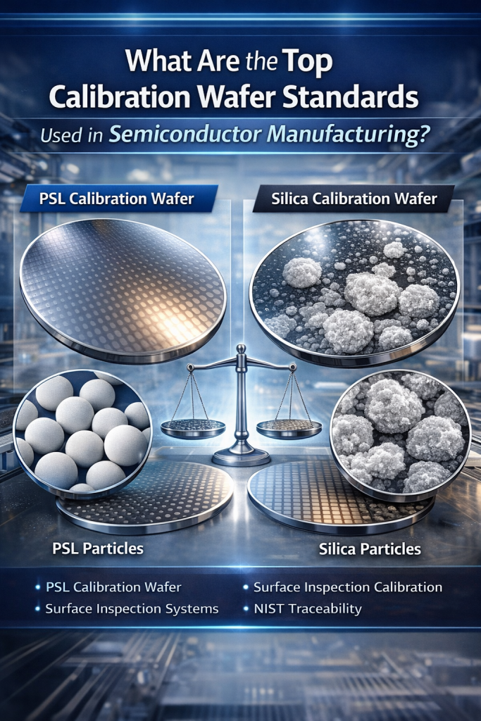
The most widely used calibration wafer standards in semiconductor manufacturing are particle calibration wafers, typically deposited with PSL (polystyrene latex) microspheres or silica microspheres, depending on the inspection technology and operating conditions.
PSL calibration wafer standards are the most commonly used reference wafers for optical inspection and surface particle metrology. These wafers are manufactured using monodisperse polystyrene microspheres deposited in controlled patterns across silicon substrates.
PSL microspheres are preferred because they offer:
These characteristics make PSL calibration wafers ideal for:
In modern fabs, PSL calibration wafers are routinely used to validate inspection sensitivity, verify recipe thresholds, and maintain consistent performance across inspection tool fleets.
Silica particle calibration wafer standards are commonly selected for high-energy inspection environments where thermal stability and laser resistance are critical.
Silica microspheres—typically ranging from 30 nm to 1 µm in diameter—are well suited for inspection tools that utilize:
Unlike polystyrene particles, silica offers enhanced resistance to laser-induced heating and deformation, making silica calibration wafers a preferred option for certain SSIS tools, advanced wafer scanners, and high-energy optical platforms.
Calibration wafer standards are used to verify and calibrate inspection tools, particle counters, and wafer scanners, ensuring accurate particle detection and consistent metrology performance in semiconductor fabs.
PSL calibration wafers offer excellent optical contrast and uniform particle size for most inspection tools, while silica calibration wafers provide improved thermal and laser resistance for high-power UV and DUV inspection systems.
High-quality calibration wafer standards are traceable to NIST reference materials, allowing measurements to be repeatable, auditable, and consistent across tools and facilities.
Yes. Calibration wafer standards can be customized by wafer size, particle material, particle size, and deposition pattern to match specific inspection tools and process conditions.
Both PSL and silica particle calibration wafer standards play a critical role in calibrating inspection systems used in:
These calibration wafers are used to support inspection tools that operate at 3 nm process nodes and below, where even minor deviations in particle detection sensitivity can impact yield and device reliability.
Today’s semiconductor manufacturers increasingly rely on custom calibration wafer standards designed to closely mirror production conditions.
Common customization options include:
By tailoring these parameters, fabs can calibrate inspection tools under conditions that closely match real process environments—improving sensitivity accuracy, tool matching, and long-term metrology confidence.
Selecting the correct calibration wafer standard directly impacts:
Well-designed, NIST-traceable calibration wafer standards enable fabs to maintain consistent process control while minimizing false alarms, measurement drift, and inspection variability.
At Applied Physics, calibration wafer standards are engineered to support the full range of semiconductor inspection and metrology applications—from routine monitoring to advanced tool qualification.
Our particle calibration wafers are designed to deliver:
These standards are trusted by semiconductor manufacturers and cleanroom operators worldwide to support accurate inspection, yield optimization, and long-term process stability.
Since 1992, Applied Physics Corporation has been a leading global provider of precision contamination control and metrology standards. We specialize in airflow visualization, particle size standards, and cleanroom decontamination solutions for critical environments.