Advanced SSIS platforms rely on high-energy DUV lasers to detect sub-30 nm defects on bare silicon wafers.
However, conventional PSL calibration spheres quickly shrink, melt, and ablate under this intense optical power, distorting measurement curves.
Inorganic silica ($\text{SiO}_2$) contamination wafer standards solve this thermal breakdown by withstanding extreme beam energy without degrading.
Switching to silica ensures accurate particle sizing, reliable tool-to-tool matching, and long-term calibration stability across modern inspection fleets.
To detect nanoscale defects on bare silicon, polished substrates, and unpatterned test wafers, inspection platforms rely on elastic light scattering (Rayleigh scattering).
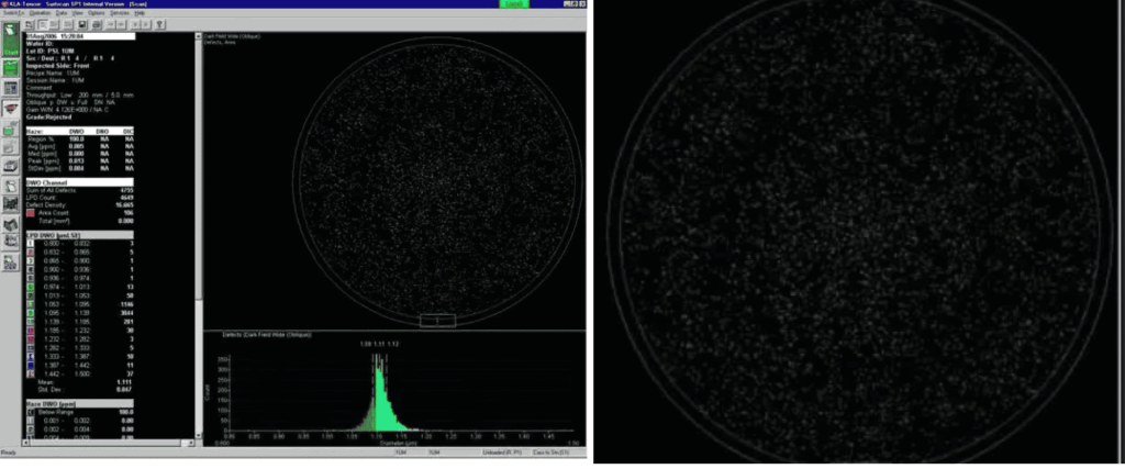
Because the scattering cross-section drops rapidly with particle diameter ($C_{scat} \propto d^6 / \lambda^4$), detecting defects smaller than 50 nm requires two system modifications.
When advanced inspection tools, such as the KLA-Tencor Surfscan SP3, SP5, SP5xp, SP7, and comparable Hitachi systems, scan a wafer, the localized energy density deposited onto the surface is substantial.
While bare silicon readily dissipates this heat, micro- and nanoscale reference particles absorb and concentrate thermal energy.
Inorganic silica nanoparticles eliminate thermal breakdown under high-power optical inspection.
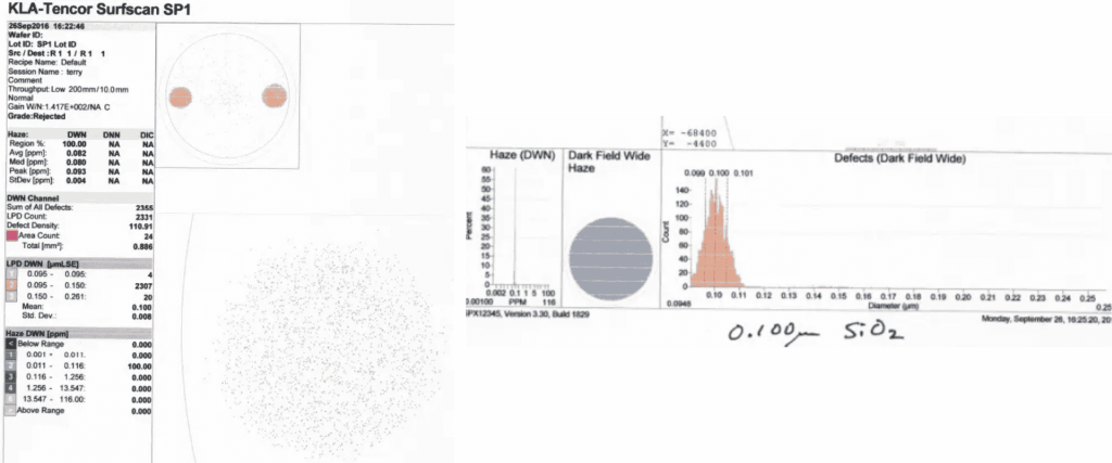
Silica features a melting temperature exceeding $1600^\circ\text{C}$.
The localized heat generated by DUV and high-intensity scanning lasers does not deform or ablate silica spheres, allowing identical spot locations to undergo multiple qualification runs without diameter loss.
The refractive index of silica ($n \approx 1.46$ in the visible-to-UV spectrum) closely mirrors common fab defects, such as real glass flakes, native oxides, and chemical-mechanical planarization (CMP) silica slurry residuals.
PSL, by contrast, has a higher refractive index ($n \approx 1.59$), which produces an artificial scattering response that differs from that of typical post-process contaminants.
Because silica particles maintain structural integrity over continuous laser exposure, engineering teams can use a single standard across multiple inspection bays, matching legacy tools (SP1, SP2) with advanced platforms (SP5, SP5xp) without standard-induced variance.
Polystyrene latex is an organic polymer with a low glass transition temperature ($T_g \approx 100^\circ\text{C}$) and a thermal decomposition threshold starting below $300^\circ\text{C}$.
When exposed to high-power, short-wavelength lasers during calibration or repeatability passes, PSL spheres exhibit distinct degradation modes.
| Feature / Metric | PSL Calibration Standards | Silica (SiO2) Contamination Standards |
| Material Base | Organic Polystyrene Latex | Inorganic Monodisperse Silica |
| Melting / Decomposition Point | $\approx 100^\circ\text{C}\ (T_g) / 300^\circ\text{C}$ (decomp.) | $> 1600^\circ\text{C}$ |
| Laser Compatibility | Low-power / Visible lasers only | High-power DUV, UV, and broad-spectrum lasers |
| Resistance to Laser Ablation | Poor (shrinks/burns under high flux) | Excellent (zero thermal deformation) |
| Multi-Pass Scan Repeatability | Low (degrades with successive passes) | High (consistent signal across repeat runs) |
| Typical Target Size Range | $20\text{ nm}$ to $100\ \mu\text{m}$ | $30\text{ nm}$ to $2.5\ \mu\text{m}$ |
| Applicable Inspection Tools | KLA SP1, SP2, legacy low-power SSIS | KLA SP3, SP5, SP5xp, SP7, Hitachi, SEM/TEM |
| Calibration Role | Basic optical size response | Precise size calibration, recipe tuning, and matching |
To maximize the utility of a silica contamination wafer standard, the deposition style should match the metrology objective.
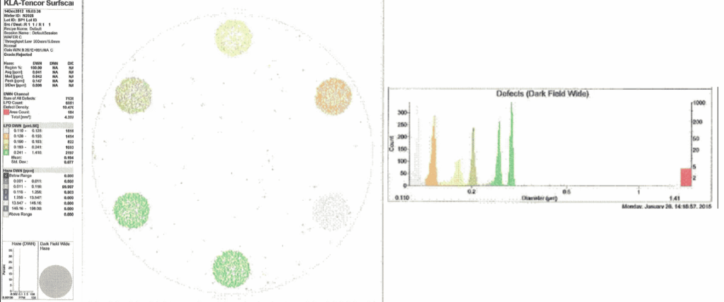
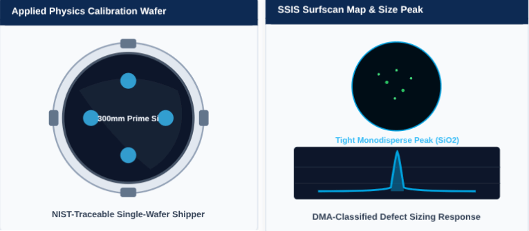
True calibration accuracy requires that the deposited silica standard consists exclusively of single, monodisperse spheres.
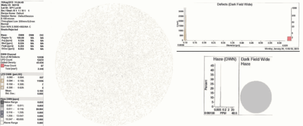
During liquid aerosolization, silica suspensions can form doublets, triplets, or carry background surfactant residue. To prevent this, standard fabrication incorporates an online Differential Mobility Analyzer (DMA).
This step ensures the resulting wafer has a tight size distribution peak without satellite clusters that could skew scattering metrics.
When upgrading inspection protocols from PSL to silica standards, keep these operational guidelines in mind.
Transitioning to monodisperse silica contamination wafer standards provides a reliable calibration path that preserves reference particle geometry, eliminates thermal scan artifacts, and maintains tool-to-tool matching across high-power inspection platforms.
Relying on delicate PSL spheres under modern high-power DUV lasers creates calibration drift and false sizing that advanced fabs simply cannot afford.
Transitioning to thermally resistant silica contamination standards prevents laser ablation at the source, mirroring the optical behavior of real process defects without degrading across repeated scans.
For metrology teams, this delivers the long-term repeatability, fleet-wide tool matching, and yield confidence required at tight process nodes.
PSL spheres consist of organic polymers with low thermal thresholds. The intense optical energy density delivered by UV/DUV lasers in modern SSIS tools heats the particles past their transition temperature, causing physical shrinkage and surface ablation during scanning.
Yes. Unlike PSL, silica has a melting point above $1600^\circ\text{C}$ and does not degrade under high-power laser irradiation. This allows the same standard to undergo repeat calibration and fleet matching runs without signal degradation.
Silica has a refractive index of approximately $1.46$, closely matching native silicon oxides and inorganic fab contaminants. PSL has an index around $1.59$. Metrology recipes must account for these optical differences when generating size calibration curves.
Silica standards can be deposited on prime silicon substrates across standard diameters, including $75\text{ mm}$, $100\text{ mm}$, $125\text{ mm}$, $150\text{ mm}$, $200\text{ mm}$, and $300\text{ mm}$ wafers, as well as borosilicate photomasks.

Enter your details below to save your shopping cart for later. And, who knows, maybe we will even send you a sweet discount code :)
Allow notifications to get real-time updates about your shopping cart and who knows, you may even receive a sweet discount code 😊