Description
The APS-T3040 Manual SMT Stencil Printer is engineered for high-precision, reliable, and cost-effective solder paste printing in PCB assembly. Designed for versatility and ease of use, this manual stencil printer is ideal for prototyping, small-batch production, and educational labs.
With robust construction and precise adjustment features, the APS-T3040 ensures consistent, repeatable results for a wide range of PCB sizes and substrate thicknesses.
Key Features
- High Precision: Achieve repeated accuracy of ±0.01mm for consistent solder paste application.
- Versatile Work Table: Accommodates PCBs up to 300×400mm, with a print area of 250×400mm.
- Adjustable Platform: Supports substrates from 0–80mm thick, with 10mm horizontal angle adjustment for optimal alignment.
- User-Friendly Operation: Manual printing mechanism with easy-to-use controls for quick setup and operation.
- Durable Construction: Built for long-term reliability in demanding environments.
- Flexible Locating: Supports both benchmark and hole shape locating modes for precise PCB positioning.
Technical Specifications
| Parameter |
Specification |
| Work Table Size |
300 × 400 mm |
| Print Size |
250 × 400 mm |
| Max Net Frame Size |
370 × 470 mm |
| Printing Method |
Manual |
| Substrate Thickness |
0–80 mm |
| Workbench Adjustment |
10 mm, Horizontal Angle |
| Printing Platform Height |
190 mm |
| Repeated Accuracy |
±0.01 mm |
| Locating Mode |
Benchmark or Hole Shape |
| Machine Dimensions |
540 × 380 × 390 mm |
| Packing Size |
660 × 500 × 280 mm |
| Net Weight |
23 kg |
| Gross Weight (Packaged) |
73 kg |
| Shipping Package Size |
108 × 80 × 52 cm |
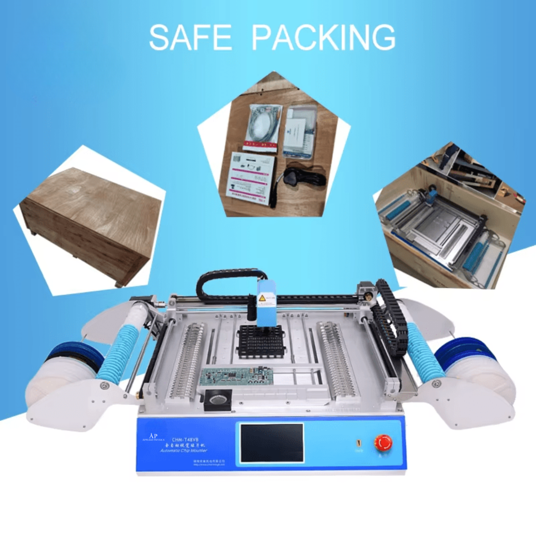
| Packing Method |
Secure Wooden Case |
Why Choose Applied Physics Semiconductor?
- Trusted US Brand: APS is a leading provider of SMT solutions, supporting American electronics manufacturers with reliable, high-quality equipment.
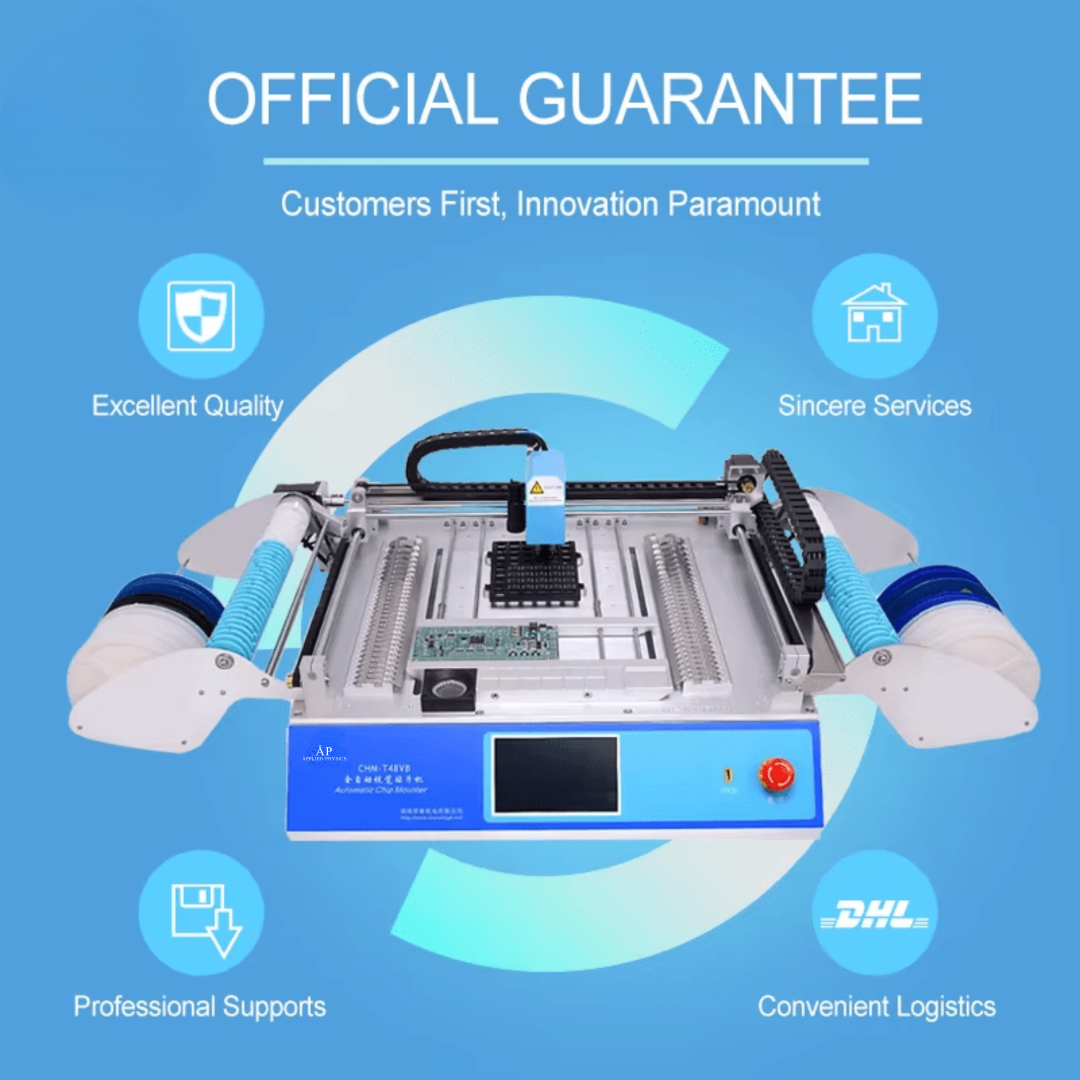
- Professional Support: Our team offers expert technical advice, training, and rapid response to ensure your success.
- Proven Performance: APS equipment is used in labs, prototyping centers, and production lines across the country.