
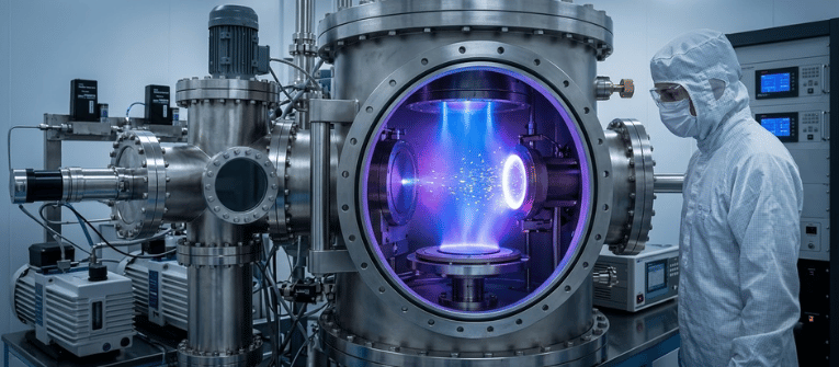
Radio Frequency (RF) sputtering stands as a cornerstone technique for depositing high-quality dielectric thin films in the semiconductor and optical industries.
Achieving maximum purity in these coatings requires a meticulous balance of plasma dynamics and chamber environmental controls to prevent contamination.
This article explores the critical optimization parameters required to refine the deposition process and achieve superior material performance.
By mastering these variables, manufacturers can ensure consistent, defect-free dielectric layers for advanced technological applications.
Unlike DC sputtering, which is limited to conductive materials, RF sputtering utilizes an alternating high-frequency current (typically $13.56 \text{ MHz}$) to prevent charge build-up on the surface of insulating (dielectric) targets.
This charge neutralization is vital because, without it, the sputtering process would cease as the target surface repels incoming ions.
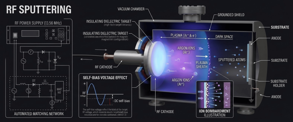
To achieve high purity, the system must not only sustain a stable plasma but also manage the self-bias voltage ($V_{dc}$) that develops on the target.
This voltage determines the energy of the ions striking the target, directly impacting the purity and density of the deposited film.
Optimizing the sputtering environment is a multi-faceted task. The following areas are the most critical for ensuring the dielectric coating remains free of impurities and structural defects.
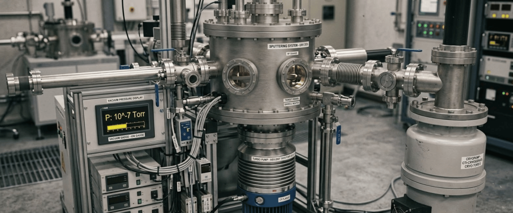
Purity begins before the plasma is even ignited. A high-purity film requires a low base pressure (typically $10^{-7} \text{ Torr}$ or better) to remove residual water vapor, oxygen, and hydrocarbons.
Even trace amounts of background gases can be incorporated into the film, altering its refractive index or electrical insulation properties.
The power density applied to the target influences the deposition rate and the kinetic energy of the sputtered atoms.

While higher power increases throughput, it can also lead to target overheating and outgassing, which introduces impurities. Gradual ramping of RF power is essential to maintain the structural integrity of ceramic or oxide targets.
The choice of inert gas (usually Argon) and its purity level (99.999% or 5 nines) is non-negotiable for high-purity outcomes.
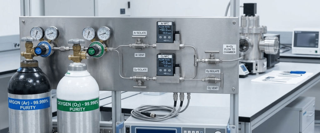
In reactive sputtering, where oxygen or nitrogen is added to create oxides or nitrides, the ratio of these gases must be controlled with extreme precision using Mass Flow Controllers (MFCs).
The table below summarizes how specific process variables affect the final quality of dielectric coatings.
| Parameter | Impact on Film Purity & Quality | Optimization Strategy |
|---|---|---|
| Base Pressure | Strongly affects interstitial impurities | Use cryopumps or turbo pumps to achieve |
| RF Power | Influences film density and stoichiometry | Optimize to balance deposition rate and defect density |
| Ar/O₂ Gas Ratio | Controls chemical composition (e.g., $SiO_2$) | Use closed‑loop MFCs for precise reactive gas control |
| Substrate Temperature | Affects adhesion and crystallinity | Maintain between and for most dielectrics |
| Target Distance | Affects uniformity and energy of arriving species | Affects the uniformity and energy of arriving species |
Contamination in dielectric coatings often stems from three main sources: the target material, the chamber walls, and the process gases. To optimize for high purity, consider.

Optimizing RF sputtering for high-purity dielectric coatings is a balance of high-end hardware and meticulous process control.
By focusing on vacuum quality, precise gas ratios, and stable power delivery, you can produce films with the exact electrical and optical properties required for cutting-edge technology.
Consistent monitoring and iterative adjustments of these parameters are the only way to ensure a repeatable, high-yield manufacturing process.
RF sputtering uses a high-frequency alternating current to prevent charge build-up on insulating (non-conductive) targets. This enables a continuous, stable plasma, which is not possible with standard DC sputtering on dielectric materials.
To achieve maximum purity, the system should reach a base pressure of at least $10^{-7} \text{ Torr}$ before deposition. This ensures that residual contaminants like water vapor and oxygen are removed from the chamber environment.
Properly optimized RF power ensures a consistent deposition rate and controls the kinetic energy of ions. Incorrect power levels can lead to target overheating and outgassing, which introduces unwanted impurities into the thin film.
Chamber seasoning involves running the sputtering process with the shutter closed for several minutes. This cleans the target surface and stabilizes the plasma environment, ensuring the actual coating deposited on the substrate is as pure as possible.