Standards & Compliance

In the high-stakes environment of semiconductor fabrication, the difference between a profitable batch and a significant financial loss often comes down to particles measured in nanometers.
As chip architectures shrink toward 2nm and 3nm nodes, the margin for error disappears.
Controlling these microscopic intruders is no longer just a maintenance task; it is the primary driver of manufacturing success.
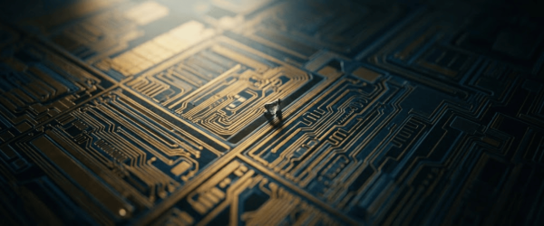
Every particle present in a cleanroom has the potential to become a killer defect. When a stray speck of dust or a chemical residue lands on a silicon wafer during the lithography or etching process, it can break a circuit line or cause a short circuit.
Higher particle counts lead directly to lower yields. When yield drops, the cost per functional chip rises, damaging the bottom line. By implementing strict particle control measures, facilities ensure that a higher percentage of wafers moving through the line reach the final packaging stage without defects.
To control particles, one must first understand where they originate. In a typical fab, contamination comes from three main sources.
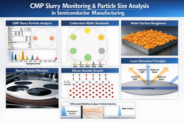
You cannot manage what you cannot measure. Modern fabs rely on Scanning Surface Inspection Systems (SSIS) to detect particles on the wafer surface. However, these tools require constant calibration to remain accurate.
Using NIST-traceable contamination wafer standards is the industry-standard method for verifying tool precision.
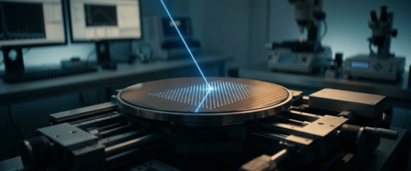
By depositing known-sized Silica or Polystyrene Latex (PSL) microspheres onto a prime silicon wafer, technicians can tune their inspection tools. This ensures that when the system flags a 20nm particle, the measurement is physically accurate, allowing for better data-driven decisions.
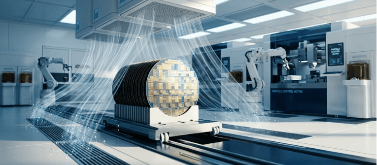
Contamination control also depends on how air moves through the cleanroom. Stagnant air pockets or turbulent zones can trap particles and deposit them directly onto sensitive equipment.
Airflow visualization, often performed using high-purity foggers, allows engineers to see the invisible currents within the fab.

By conducting smoke studies, teams can verify that laminar flow hoods and ceiling filter units are pushing contaminants away from the production line and toward the floor vents. This proactive mapping of air movement prevents particles from ever reaching the wafer surface.
This table shows how even extremely small particles can damage modern technology nodes (chips).
| Technology Node | Critical Particle Size (nm) | Impact on Yield |
|---|---|---|
| 10 nm Node | > 5 nm | Obstruction in circuit connectivity |
| 7 nm Node | > 3.5 nm | High resistance and heat issues |
| 5 nm Node | > 2.5 nm | Short circuits and total chip failure |
| 3 nm / 2 nm Node | > 1.5 nm | Fatal killer defects and yield loss |
The final pillar of yield improvement is stabilizing the environment. High-Efficiency Particulate Air (HEPA) and Ultra-Low Penetration Air (ULPA) filters must be monitored for leaks or saturation. Beyond air filtration, maintaining consistent pressure differentials between rooms prevents cross-contamination.
If a gowning room has higher pressure than a sterile suite, dirty air will naturally flow into the sensitive area. Automated monitoring systems ensure these pressure gradients remain intact 24/7.
Improving semiconductor yield through particle control requires a combination of advanced hardware, rigorous calibration, and constant vigilance.
By focusing on the elimination of killer defects through better inspection standards and optimized airflow, manufacturers can protect their wafers, increase their output, and maintain a competitive edge in the global electronics market.
Managing particles is vital because even a tiny contaminant can bridge electrical paths on a wafer. As chip sizes decrease, even sub-microscopic dust can cause massive production failures and lower the total yield.
A killer defect is a particle or flaw that causes a chip to malfunction completely. These defects often settle during the lithography phase, breaking the delicate circuit patterns required for the semiconductor to operate.
These standards provide a reference point for inspection machines. By using known particle sizes, manufacturers can ensure their sensors are sensitive enough to find contaminants before they ruin an entire batch of wafers.