

As semiconductor fabrication moves beyond the 3nm node and enters the Angstrom era, the margin for error in contamination control has effectively vanished.
At these scales, a single particle smaller than 20 nanometers can result in a catastrophic killer defect on a wafer.
To maintain high yield rates, metrology tools must be calibrated with absolute precision.
This is where sub-20nm PSL (Polystyrene Latex) Spheres become the industry standard for accuracy and repeatability.
For decades, the industry measured process nodes in nanometers ($nm$). However, with the advent of 2nm and 18A (1.8nm) processes, the focus has shifted to the Angstrom ($Å$) scale ($1nm = 10Å$).
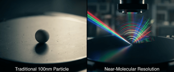
In this ultra-fine manufacturing environment, traditional calibration particles are often too large to validate the sensitivity of modern Laser Surface Scanning Systems and Differential Mobility Analyzers (DMA).
Sub-20nm PSL spheres provide the near-molecular resolution required to ensure that inspection equipment can differentiate between actual defects and background noise.
Calibration is only as good as the reference material used. Sub-20nm PSL spheres are preferred in high-end metrology for several technical reasons.
These spheres are synthesized with an extremely narrow size distribution (monodisperse), ensuring that every particle in a solution is virtually identical in diameter.
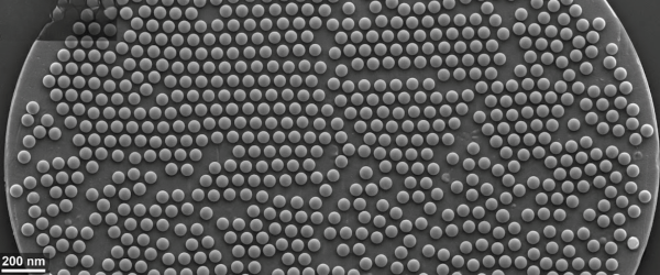
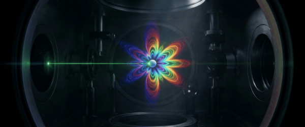
The perfect spherical shape allows for predictable light-scattering patterns (Mie Theory), which is critical for calibrating optical particle counters.
High-quality PSL spheres are calibrated against National Institute of Standards and Technology (NIST) reference materials, providing an unbroken chain of documentation for ISO 14644 compliance.

Calibrating at the sub-20nm level introduces unique physics-based challenges. At these sizes, particles behave differently due to increased Brownian motion and surface energy.
The following table illustrates the typical application ranges for various calibration particle sizes in the current semiconductor landscape.
| Particle Size Range | Primary Application | Metrology Tool Focus |
|---|---|---|
| 80nm, 100nm | Legacy Node Inspection | Standard Optical Particle Counters |
| 30nm, 50nm | 5nm & 7nm Process Control | High‑Sensitivity LSPS |
| Sub‑20nm (10nm, 19nm) | 2nm / Angstrom Era Research | Scanning Electron Microscopy (SEM) / DMA |
| Sub‑10nm | Molecular Contamination Study | Advanced Aerosol Spectrometers |
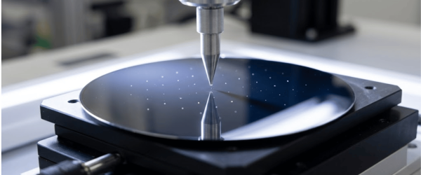
To achieve a #1 ranking in production yield, facilities must use these spheres to create Calibration Curves. By depositing sub-20nm PSL spheres onto a silicon wafer in a controlled pattern (Spot Deposition), technicians can map the response of inspection lasers across the entire wafer surface.
This process ensures that when the system scans a production wafer, it can accurately identify a 15nm contaminant versus a 10nm surface irregularity.
The transition to Angstrom-scale manufacturing is not merely a decrease in size; it is a fundamental change in how we perceive and measure matter.
Sub-20nm PSL spheres are the foundational tools that allow this transition to happen safely and profitably.
By providing a reliable, NIST-traceable reference point, these particles ensure that the metrology tools of today are ready for the chips of tomorrow.
As chip nodes shrink to 2nm and below, even the smallest particles can cause electrical shorts. Sub-20nm PSL spheres allow metrology tools to detect these microscopic killer defects that larger particles would miss during the inspection process.
Polystyrene Latex (PSL) spheres are perfectly round and uniform in size. This consistency allows lasers in inspection systems to reflect light predictably, making it easy for engineers to set accurate baselines for equipment sensitivity and performance.
Moving from nanometers to Angstroms requires a significant increase in precision. Sub-20nm spheres act as a vital reference point, providing the high-resolution data needed to validate the performance of next-generation scanning systems and lithography tools.
NIST traceability ensures that the size of the PSL spheres is verified against recognized international standards. This documentation is essential for maintaining ISO 14644 compliance and ensuring consistent quality control across different semiconductor fabrication facilities.
