
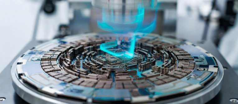
Semiconductor manufacturing is pushing physical limits.
As fabrication drops below the 5-nanometer (nm) threshold, reaching 3nm and 2nm nodes, the methods used to measure and inspect silicon wafers must adapt.
Metrology, the science of measurement, is facing severe technical bottlenecks. Accurately detecting defects and measuring critical dimensions (CD) at this scale requires entirely new approaches to optical and electron-beam inspection.
Here is an analysis of the primary metrology challenges encountered at the sub-5nm level and how the industry is addressing them.
At older nodes, transistors were largely planar. Sub-5nm designs rely on complex three-dimensional structures like Gate-All-Around (GAA) field-effect transistors and nanosheets.

Metrology tools must now measure hidden features, undercuts, and high-aspect-ratio trenches. Traditional 2D top-down scanning electron microscopy (CD-SEM) cannot accurately capture depth or identify buried defects in these multi-layered structures. Engineers need instruments capable of penetrating opaque layers without destroying the wafer.
Optical metrology offers high throughput, scanning wafers on the production line. However, optical systems lack the resolution to detect nanometer-scale defects.
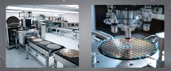
Conversely, e-beam inspection provides the necessary high resolution to see sub-5nm defects but operates far too slowly for high-volume manufacturing (HVM). Balancing the speed of optical tools with the precision of e-beam systems remains a major operational hurdle for fabrication facilities.
Extreme Ultraviolet (EUV) lithography creates incredibly fine patterns. The photoresist materials used in EUV are thin, fragile, and highly sensitive.
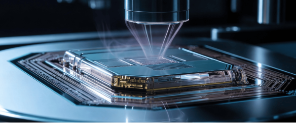
When metrology tools, particularly electron beams, interact with these delicate layers to take measurements, the energy can cause the resist to shrink or deform. Measuring the exact dimension without physically altering the structure is difficult.
With features shrinking to the atomic level, aligning multiple semiconductor layers exactly on top of each other is mandatory.
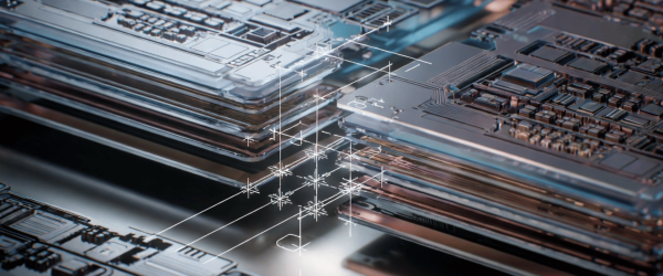
A misalignment of just one or two nanometers causes an Edge Placement Error (EPE), leading to total device failure. Metrology systems must measure layer-to-layer overlay with sub-nanometer accuracy across the entire surface of the 300mm silicon wafer.
To overcome measurement uncertainties at the sub-5nm level, the baseline accuracy of inspection tools must be absolute. Surface Scanning Inspection Systems (SSIS) and particle counters require exact calibration to ensure accurate data output.
Using high-quality calibration standards, such as Polystyrene Latex (PSL) spheres and silica wafer standards, ensures that metrology equipment accurately identifies killer defects versus harmless background noise. At 3nm nodes, even a 10nm particle can destroy a transistor. Regular tool calibration with certified size standards is the only method to maintain reliable baseline measurement data.
| Metrology Parameter | Traditional Node (14nm – 7nm) | Next‑Gen Sub‑5nm Node | Technical Solution |
|---|---|---|---|
| Transistor Structure | FinFET (Planar / 3D) | GAA (Gate‑All‑Around) / Nanosheets | 3D Modeling & CD‑SAXS |
| Inspection Resolution | Optical & Standard SEM | Sub‑nanometer E‑beam | Multi‑beam Electron Inspection |
| Measurement Depth | Surface‑level inspection | High‑Aspect‑Ratio (HAR) Trenches | X‑ray Metrology & Hybrid Probe |
| Beam Sensitivity | Stable Photoresist | Fragile EUV Photoresist | Low‑voltage / Cryo‑EM |
| Alignment Tolerance | 2nm – 3nm Overlay | < 1nm Edge Placement Error (EPE) | AI‑driven Overlay Analytics |
| Calibration Standard | Standard PSL Spheres | Ultra‑fine Silica / PSL Standards | Certified Wafer Calibration Tools |
Because no single tool can measure everything at the sub-5nm level, fabrication facilities are adopting hybrid metrology.
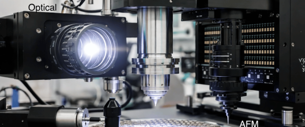
This process involves combining measurement data from multiple sources, such as optical scatterometry, atomic force microscopy (AFM), and X-ray metrology (CD-SAXS). By feeding this combined data into advanced analytics software, engineers can reduce measurement noise, eliminate blind spots, and achieve a highly accurate 3D profile of the wafer.
Shrinking semiconductor nodes guarantee that metrology will become more difficult.
Overcoming the sub-5nm barrier requires moving past traditional top-down inspection, implementing strict calibration protocols with certified wafer standards, and adopting hybrid measurement techniques.
Maintaining high production yield at 3nm and beyond depends entirely on what manufacturers can accurately measure and verify.
Traditional metrology tools primarily scan surface-level features. New 3D designs, such as Gate-All-Around (GAA) and nanosheets, contain hidden vertical layers and deep trenches. These internal features are often invisible to standard optical tools, requiring advanced X-ray or hybrid metrology to verify internal dimensions.
The primary bottleneck is balancing resolution with production speed. While electron-beam (e-beam) technology offers the high resolution necessary to detect sub-5nm defects, it is significantly slower than optical inspection. Finding a way to achieve high-resolution imaging without slowing down the manufacturing line is a major industry challenge.
At the sub-5nm scale, the margin for error is nearly zero. Even a 10nm particle can lead to a killer defect that destroys a transistor. Regular calibration using certified wafer standards and PSL spheres ensures that inspection equipment remains accurate and can distinguish between microscopic noise and actual defects.