
The semiconductor industry has successfully bypassed the physical scaling limitations of planar (2D) NAND flash memory by moving into the vertical dimension.
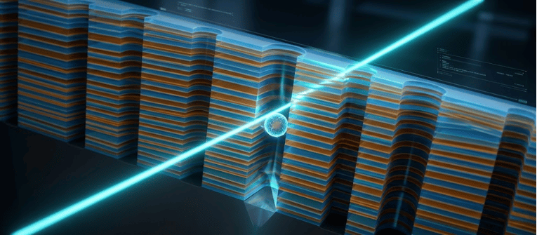
3D NAND technology relies on stacking alternating thin films of materials, typically insulating oxide ($\text{SiO}_2$) and sacrificial nitride ($\text{Si}_3\text{N}_4$) layers on top of a silicon substrate.
Through a series of advanced photolithography, deep reactive-ion etching (DRIE), and chemical vapor deposition (CVD) steps, columns of vertical memory cells are formed simultaneously.
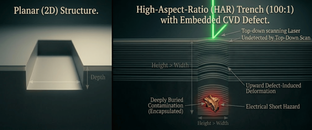
However, as manufacturers scale memory density vertically to achieve 232, 280, or more than 300 layers, the physical profile of the structures shifts drastically.
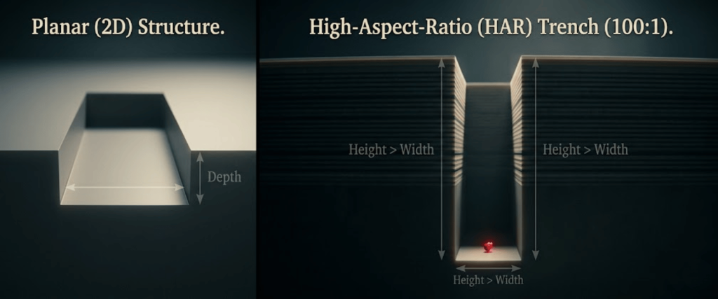
The vertical holes or channel trenches exhibit unprecedented High-Aspect-Ratio (HAR) profiles, frequently exceeding depth-to-width ratios of 70:1 or 100:1.
At these extreme geometries, microscopic contamination that was once considered negligible on planar wafers now causes catastrophic structural failure and total device yield loss.
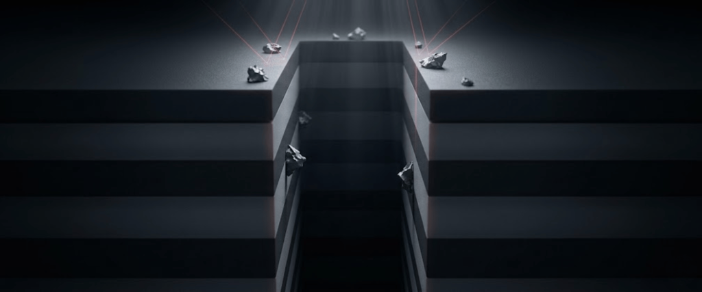
Microscopic particle detection in 3D NAND scaling becomes highly challenging because memory holes are very deep and narrow. Inside these high-aspect-ratio trenches, particles can easily hide, which prevents standard top-down inspection tools from detecting them.
As NAND layers continue to increase, the risk of contamination also rises. Small particles trapped in buried layers can cause device defects, shorts, and yield loss. That is why advanced metrology, contamination control, and accurate calibration standards are essential for 3D NAND manufacturing.
The primary structural challenge in modern 3D NAND manufacturing is the structural depth of the memory holes. A typical memory hole must penetrate through multiple micrometers of alternating film stacks with absolute vertical uniformity.
This extreme geometry exacerbates defect capturing and detection mechanisms in two fundamental ways.
Microscopic particles can settle on the sidewalls of deep memory holes during deposition or etching. Because standard optical inspection uses top-down viewing, these particles may stay hidden inside narrow channels.
In 3D NAND, particles deposited during early CVD steps can become buried as more layers are added.
Once buried, they are difficult to detect and can later cause defects, line distortions, or electrical shorts during etching.
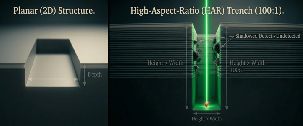
Traditional inspection tools struggle with 3D NAND due to the extreme depth and narrow width of memory holes.
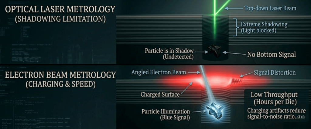
Optical systems often miss very small particles since their signals become weak and are lost in background noise from complex film stacks and sidewalls. Electron beam inspection offers better resolution, but it is too slow for full-wafer inline production.
| Metrology Technique | Detection Capability Limit | Throughput Characteristics | Primary Limitation in 3D NAND |
|---|---|---|---|
| Optical Laser Scattering | ~15 nm to 20 nm (on planar surfaces) | High (full wafer in minutes) | Severe geometric shadowing; cannot resolve particles inside high-aspect-ratio trenches. |
| Electron Beam (EBI) | ~1 nm to 3 nm | Very low (hours per die/wafer) | Charging effects and poor scalability for inline mass production. |
| Deep UV (DUV) Optical | ~10 nm to 15 nm | Medium | Complex optical interference from alternating film layers. |
To overcome the optical noise and geometrical constraints of 3D NAND scaling, wafer inspection tools must be calibrated to the absolute physical limits of performance.
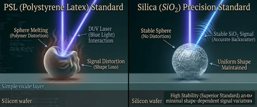
This requires the deployment of highly uniform Calibration Wafer Standards. By depositing precisely sized spherical particles onto specialized monitor wafers, contamination engineers can map the exact detection thresholds of their inspection systems.
The transition to hyper-scaled 3D NAND architectures has permanently shifted the rules of semiconductor contamination management.
High-aspect-ratio channels introduce physical, structural, and optical dynamics that render classic planar inspection models insufficient.
As features shrink below the sub-20nm threshold, the combination of advanced optical tuning, rapid-throughput electron beam inspection, and flawless tool calibration via stable Silica and PSL size standards represents the only viable pathway to sustaining high-volume yields in next-generation memory manufacturing.
Optical laser scattering tools rely on top-down light paths that suffer from severe geometric shadowing in ultra-high layer stacks. As aspect ratios exceed 70:1, light cannot effectively penetrate to the bottom of deep, narrow memory holes, leaving sub-micron contamination completely hidden from surface inspection scanners.
Rayleigh scattering principles dictate that the intensity of scattered light drops exponentially with the sixth power of a particle’s diameter. When microscopic contamination shrinks below the 20nm threshold, the light signal becomes too weak to distinguish from the background noise and optical haze of alternating oxide-nitride layers.
Silica ($\text{SiO}_2$) spheres provide high thermal and structural stability under intense Deep UV lasers, preventing shape distortion during automated scanning. Furthermore, their refractive index closely mimics the optical properties of actual process defects generated inside plasma etching and deposition chambers.
Inside narrow vertical channels, gas transport enters the Knudsen diffusion regime, where sub-micron particles collide more frequently with structural sidewalls than with other gas molecules. This phenomenon, coupled with localized electrostatic forces during plasma steps, increases the probability of permanent particle adhesion via van der Waals forces.