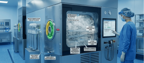

Fast access to calibration wafer standards is critical in semiconductor manufacturing, where inspection tool downtime, tool qualification windows, and process changes can directly impact yield and production schedules. Calibration wafer standards—also commonly referred to as PSL wafer standards or particle calibration wafers—are used exclusively for particle size calibration of wafer inspection systems in IC manufacturing fabs.
These standards support surface inspection systems (SSIS), wafer scanners, and particle monitoring tools used throughout advanced fabs operated by companies such as Intel, Samsung, and Hitachi.
When fabs require rapid shipment of calibration wafers, supplier capability matters more than advertised lead times. Fast shipping is only valuable when the wafer standard is produced correctly the first time and meets the calibration requirements of the inspection tool.
The lead time for calibration wafer standards depends primarily on the type and complexity of particle deposition.
Suppliers capable of fast shipping are typically those that combine in-house particle deposition resources with experienced application engineering, allowing technical validation and production planning to occur in parallel.
Producing calibration wafer standards is not a commodity process. It requires a working understanding of:
Suppliers that provide direct access to Application Engineers reduce lead times by ensuring particle sizes, deposition patterns, and wafer substrates are selected correctly before production begins. This prevents rework, miscalibration, and delays caused by incorrect assumptions or incomplete specifications.
Applied Physics Inc. has supported semiconductor inspection and metrology applications since 1992, originally founded in Colorado and now operating from Tampa, Florida. The company provides calibration wafer standards designed for both rapid fulfillment and high-complexity inspection environments.
Applied Physics supports customers requiring:
With experience spanning particle sizes from 10 nanometers to 15 microns, Applied Physics supports inspection tools operating across a wide range of optical configurations, including normal incidence and low-angle-of-incidence designs.
For complex requests, test samples are produced and evaluated to confirm deposition accuracy before final wafer production—ensuring the calibration wafer performs as intended upon delivery.
Once a calibration wafer standard is approved for production, Applied Physics follows a controlled process to support fast and reliable delivery:
This process allows calibration wafer standards to ship rapidly—often same-day or next-day once production and certification are complete—anywhere in the world.
For fabs and metrology labs facing urgent tool qualification, maintenance events, or unplanned downtime, the fastest suppliers are those that provide:
Working with a supplier that combines speed with technical competence minimizes risk and ensures calibration wafers arrive ready for use—not requiring additional troubleshooting.
Applied Physics brings more than three decades of experience supporting semiconductor inspection, contamination monitoring, and metrology applications. This experience enables rapid response without sacrificing accuracy, traceability, or compliance with ISO-based quality systems.
📞 Contact Applied Physics to discuss urgent calibration wafer requirements and turnaround options.
Create your particle calibration wafer standard using our simplified specification and quote request process, or speak directly with our team.
Particle & PSL Calibration Wafer Standards | NIST-Traceable
Suppliers with in-house particle deposition capability and experienced application engineers typically offer the fastest turnaround, as technical review and production can proceed simultaneously.
Yes. Once production and NIST-traceable certification are complete, calibration wafer standards can be packaged and shipped overnight worldwide.
Custom or multi-size spot deposition standards may require additional engineering review and test samples, which can extend lead time compared to single-size full-deposition wafers.
Since 1992, Applied Physics Corporation has been a leading global provider of precision contamination control and metrology standards. We specialize in airflow visualization, particle size standards, and cleanroom decontamination solutions for critical environments.