

In the world of semiconductor manufacturing, precision isn’t just a goal; it is the baseline.
As the industry pushes toward increasingly smaller nodes, the tolerance for overlay error (the misalignment between successive circuit layers) has shrunk to just a few nanometers.
Even a microscopic shift can result in catastrophic electrical shorts, opens, and significant yield loss.
Troubleshooting these defects requires a transition from basic calibration to a systematic, data-driven approach.
This guide explores advanced strategies for identifying and correcting misalignment in modern lithography steppers and scanners.
Before diving into repairs, it is essential to distinguish between the types of errors appearing on the wafer.
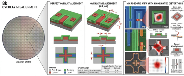
Misalignment is rarely a single-source problem; it is often a combination of linear and non-linear distortions.
These are global errors where the entire pattern is shifted (X or Y axis) or rotated relative to the previous layer.
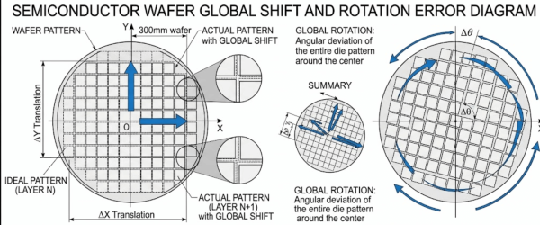
These are typically the easiest to correct using software offsets, but often point to issues with wafer-stage initialization.
If the pattern size doesn’t match the underlying layer, you likely have a magnification issue.
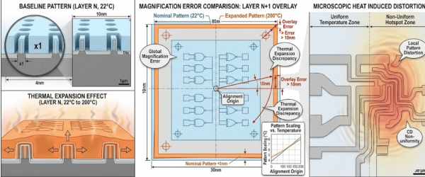
This often stems from wafer or lens thermal expansion or from lens heating during high-volume production runs.
In advanced nodes, trapezoid or bowing effects occur.
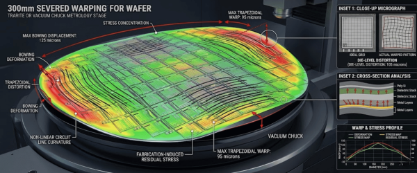
These non-linear errors are frequently caused by wafer warpage or mechanical stresses introduced during previous deposition or annealing steps.
When an overlay excursion occurs, follow this tiered diagnostic path to isolate the root cause.
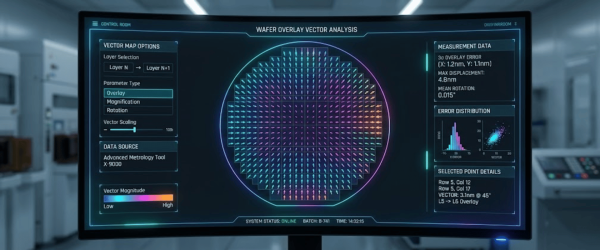
Don’t touch the hardware until you’ve analyzed the Overlay Vector Map.
The wafer stage must move with atomic-level repeatability. Troubleshooting should focus.
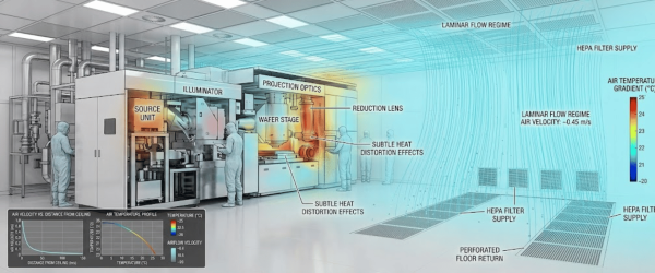
Lithography tools are incredibly sensitive to their surroundings.
Once the source is identified, apply these high-level corrections.
| Error Type | Likely Root Cause | Advanced Correction |
|---|---|---|
| Grid Non‑Orthogonality | Stage mirror misalignment | Re‑calibrate stage X/Y orthogonality constants |
| Intra‑field Rotation | Reticle stage error | Synchronize reticle and wafer stage scan speeds |
| Local Overlay Shift | Wafer stress/warpage | Implement feed‑forward correction based on pre‑exposure wafer mapping |
| Consistent X/Y Offset | Pre‑alignment sensor drift | Re‑zero the Off‑Axis Alignment (OAA) sensors |
Advanced troubleshooting is most effective when paired with a robust preventative maintenance (PM) schedule.
Mastering misalignment defects requires a blend of mechanical intuition and rigorous data science.
By categorizing errors into global and local distortions and utilizing a phased troubleshooting approach, fabs can maintain high yield even at the most demanding process nodes.
Misalignment, or overlay error, is typically caused by mechanical issues like wafer stage initialization failures, thermal expansion from lens heating, or microscopic contamination on the wafer chuck. Even a 0.1°C change in cleanroom temperature can shift the alignment.
Engineers use Overlay Vector Maps to identify the pattern. If all vectors point in one direction, it is a global translation error. If the vectors spiral or appear trapezoidal, it indicates a local distortion caused by wafer warpage or reticle stage synchronization issues.
The most effective prevention is a combination of regular stage calibration and real-time monitoring. Implementing feed-forward corrections and ensuring alignment marks are not degraded by previous etching or polishing steps will significantly reduce drift during high-volume production.