
In the hyper-competitive world of semiconductor manufacturing, the difference between a high-yield production run and a multi-million dollar loss is measured in nanometers.
As the industry pushes the boundaries of Moore’s Law, moving into sub-5nm process nodes, the size of a killer defect has shrunk to a point where even the most advanced inspection tools can struggle to differentiate between a particle and a surface irregularity.
To maintain precision, fabrication facilities (fabs) rely on Wafer Calibration Standards.
These specialized tools are the gold yardsticks of the semiconductor world, ensuring that the lasers and sensors used to inspect silicon wafers are accurate, repeatable, and reliable.
In older manufacturing nodes, a 50nm particle might have been negligible.

In modern EUV (Extreme Ultraviolet) lithography processes, that same particle is a catastrophic defect that can short-circuit a transistor.
A Wafer Calibration Standard is a prime silicon wafer that has been intentionally deposited with highly uniform particles of a known size.
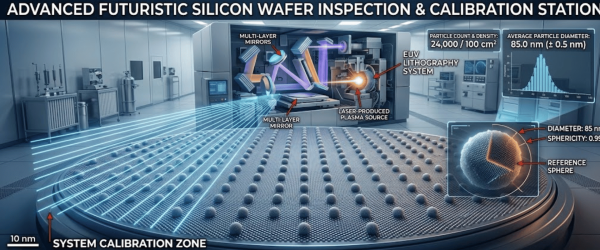
These particles act as a reference point for Surface Scanning Inspection Systems (SSIS), such as those produced by KLA, Applied Materials, and Hitachi.
PSL spheres have been the industry standard for decades. They offer excellent size uniformity and are available in a wide range of NIST-traceable sizes.
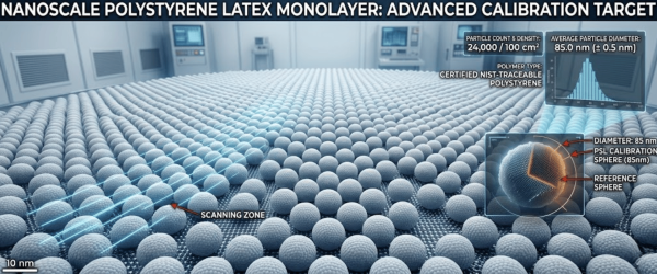
They are primarily used to calibrate the sizing accuracy of scanners.
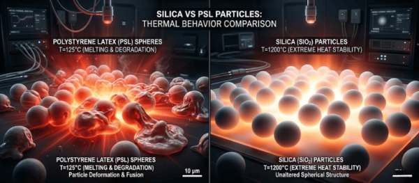
As nodes shrink, Silica microspheres are becoming increasingly popular. Unlike PSL, which is a polymer, Silica has a refractive index closer to the actual contaminants found in a production environment.
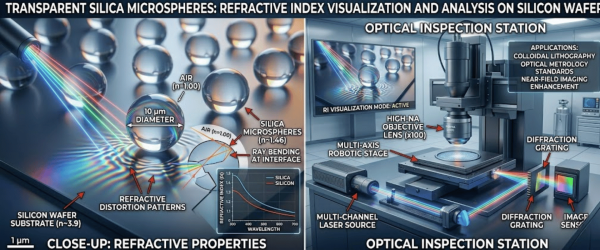
This makes Silica standards superior for tuning tools to recognize real-world defects during the cleaning and etching phases.
The implementation of advanced calibration standards directly impacts the bottom line of a semiconductor fab through three primary mechanisms:
If an inspection tool is not properly calibrated, it may filter out small particles, assuming they are background noise.

By using a Full Deposition Wafer Standard, engineers can verify the tool’s sensitivity across the entire surface, ensuring that even the smallest killer defects are flagged before the wafer moves to the next expensive lithography step.
Over-sensitive tools can flag harmless surface variations as defects, leading to ghost errors. This results in unnecessary wafer cleaning cycles or, worse, the scrapping of perfectly good wafers.
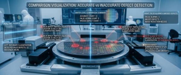
Calibration standards enable precise binning, in which the tool is taught exactly what constitutes a defect worth stopping the line for.
In high-volume manufacturing, a single fab might utilize dozens of inspection scanners. If Tool A is slightly more sensitive than Tool B, the data becomes unreliable.

Using NIST-traceable calibration standards ensures that every machine in the fleet is synchronized to a single global measurement standard.
For a calibration standard to be effective, its accuracy must be beyond reproach. Leading providers like Applied Physics ensure that their microspheres are traceable to the National Institute of Standards and Technology (NIST).

This traceability provides the documented proof required for ISO quality audits and ensures that the measurements taken on the fab floor are scientifically defended.
The industry is currently looking toward the Angstrom Era.
Advanced Wafer Calibration Standards are the unsung heroes of the semiconductor revolution.
By providing a reliable, repeatable reference for inspection tools, they allow manufacturers to navigate the transition to next-gen nodes with confidence.
In an era where a single particle can compromise an entire batch of microchips, the precision provided by these standards is not just an advantage; it is a necessity for survival in the global electronics market.
While PSL (Polystyrene Latex) is excellent for size calibration, Silica microspheres have a refractive index that more closely mimics the actual contaminants found in a real-world fab environment. As nodes shrink to 3nm and below, using Silica allows engineers to tune their inspection tools to detect real-world defects more accurately, reducing the interference caused by surface haze.
To maintain high yield, calibration should be performed at regular scheduled intervals and whenever a tool shows signs of drift. Frequent calibration with NIST-traceable standards ensures that every scanner in the facility is synchronized, preventing killer defects from slipping through the cracks and saving millions in potential scrapped wafers.