
Last Updated: August 4, 2026
Semiconductor fabrication process control tools are non-negotiable infrastructure in modern chip manufacturing. At sub-10nm nodes, a single deviation in process parameters can cascade into millions of dollars in scrap wafers. The economics are brutal: a single wafer costs $10,000-$50,000 to produce. With 500+ chips per 300mm wafer, a 1% yield loss translates to $1.5M per production run. Process control tools catch problems before they become catastrophic losses.
This guide covers the hardware, software, and methodologies that separate world-class fabs from the rest: statistical process control frameworks, advanced process control strategies, metrology systems, and AI’s emerging role in fab automation. By the end, you’ll understand what tools your facility needs and how to implement them without disrupting production.
Real-time monitoring only matters if you know what to do with the data. Statistical process control transforms raw measurements into actionable decisions by establishing control limits based on historical process behavior, then flagging measurements outside those bounds.
SPC’s foundation is straightforward: measure a parameter repeatedly, calculate mean and standard deviation, then set control limits at ±3 sigma from the mean. Any measurement beyond those limits triggers investigation. The power lies in detecting trends before they become failures, a slow drift in deposition temperature becomes visible when five consecutive measurements trend upward.
Modern SPC systems ingest data from dozens of sensors simultaneously: chamber pressure, temperature, gas flow rates, RF power, deposition rates, etch rates. The software calculates control statistics in real-time and generates alerts when parameters drift. Applied Physics has deployed metrology solutions that integrate directly with fab data networks, feeding measurement data into SPC engines without manual intervention.
The challenge is distinguishing signal from noise. Environmental vibration, sensor drift, or transient equipment behavior can trigger false alarms. Effective SPC systems use rational subgrouping, grouping measurements to isolate true process variation from measurement system noise.
Pro Tip Set SPC control limits based on at least 25-30 subgroups of historical data. Limits from fewer samples generate excessive false alarms, leading teams to ignore legitimate warnings.
Process variability is the enemy of yield. Even when a process is “in control,” natural variation still produces devices with different characteristics. Reducing this variability directly improves yield and reduces cost per die.
The real challenge emerges with multiple identical tools running the same process. Subtle differences in chamber geometry, electrode wear, gas distribution, and thermal profiles cause Tool A to run 2-3°C hotter than Tool B. This chamber-to-chamber variation compounds across the fab, creating a wider distribution of outcomes than a single tool’s natural variation.
Advanced fabs tackle this through chamber matching: characterizing each tool’s unique signature and adjusting set points to compensate. A tool running hot gets its temperature set point lowered. One with uneven gas distribution gets its showerhead geometry adjusted. The goal is making all tools produce identical output despite physical differences.
SPC across tool sets requires centralized data collection and cross-tool analysis. You need to see whether Tool A and Tool B are drifting relative to each other, which requires fab-wide tool communication and integration.
Advanced process control moves beyond monitoring what happened to predicting and preventing problems before they occur. At sub-10nm nodes, the process window is so narrow that reactive control is too slow.
Feed-forward control adjusts the current run based on measurements from previous runs. If Run 1 produced wafers with slightly thinner films, Run 2 automatically increases deposition time. The system learns the relationship between process inputs and outputs, then compensates for drift.
Run-to-run (R2R) control is the practical implementation. After each wafer completes a process step, metrology measurements are taken. The APC system analyzes those measurements, calculates an adjustment to process parameters, and applies it to the next wafer. This feedback loop automatically compensates for tool drift, material variation, and environmental changes.
R2R control relies on process models, equations describing how changing a parameter affects an outcome. Building accurate models requires design-of-experiments (DOE) studies that systematically vary parameters and measure outcomes. A typical DOE for deposition might vary temperature, pressure, and gas flow rate across operating ranges, producing 20-50 experimental runs.
Watch Out Inaccurate process models are worse than no model. A flawed model makes systematic adjustments in the wrong direction, driving the process further from target. Validate models on new data before deploying in production.
When 10 identical deposition chambers run the same process, you expect identical results. Chamber A deposits films 3% thicker than Chamber B due to subtle gas distribution differences. Chamber C runs 15°C cooler because its thermal profile differs.
Chamber matching corrects these differences through characterization and compensation. Each chamber runs a standard test, and resulting thickness is measured. Chambers running thick get deposition time reduced; chambers running thin get it increased. The goal is making all chambers produce identical results.
This requires tool communication infrastructure. Each chamber reports characterization data to a central database. The fab-wide control system analyzes that data, calculates compensation adjustments, and pushes new set points back to each tool. Modern fabs use SECS/GEM (Semiconductor Equipment Communications Standard / Generic Equipment Model) to standardize communication between tools and control systems, allowing the control system to read parameters, retrieve data, and send updated set points without manual intervention.
Measurement is the foundation of process control. You cannot control what you cannot measure. In-line metrology systems perform measurements on wafers during production, providing real-time feedback that drives SPC and APC.
Optical metrology dominates in-line measurement because it’s fast, non-destructive, and doesn’t require wafer handling. Spectroscopic reflectometry measures film thickness by analyzing light reflection off thin films. Scatterometry measures critical dimensions by analyzing light scattering from patterned features.
The advantage is throughput: modern systems measure wafers in seconds. The limitation is that optical measurements depend on material optical properties. Measuring transparent oxide films is straightforward; measuring through opaque layers or in high-aspect-ratio structures is harder.
Electron beam (e-beam) inspection provides higher resolution and can measure features optical systems cannot access. E-beam tools focus a narrow electron beam on the wafer surface and analyze secondary electrons that bounce back, achieving sub-nanometer resolution.
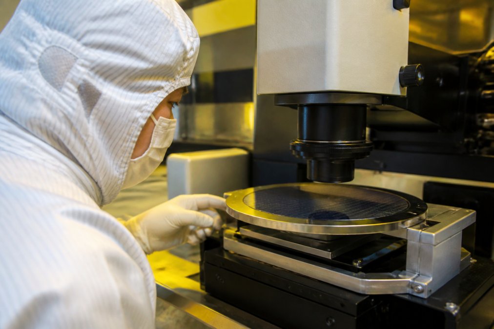
Semiconductor fabrication technician examining wafer samples under advanced inspection equipment in a cleanroom environment with controlled lighting and precision instruments
The trade-off is speed. E-beam tools measure one small region at a time, making them much slower than optical systems. A typical e-beam tool measures 10-20 wafers per hour versus 200+ for optical tools. E-beam tools are typically used for review and failure analysis, not high-volume in-line monitoring.
Every measurement system needs calibration using reference standards that verify the tool is measuring correctly. In semiconductor metrology, calibration wafers with known film thicknesses or critical dimensions serve as these standards.
Applied Physics manufactures calibration wafer standards for 300mm, 200mm, 150mm, and 125mm wafer sizes, traceable to NIST (National Institute of Standards and Technology) reference materials, ensuring measurement uncertainty is quantified and documented. Without proper calibration standards, you cannot verify that metrology tools are measuring correctly.
Calibration should happen frequently, daily or weekly depending on tool stability and measurement criticality. Tools that drift slowly gradually produce incorrect results without frequent recalibration. A film thickness measurement off by 5% might cause a 10% yield loss in downstream processing.
Raw measurement data means nothing without analysis and action. Yield management software aggregates data from metrology tools, SPC systems, and tool parameters, then identifies patterns explaining yield loss.
Yield management systems ingest terabytes of data daily from every wafer, tool, and process step. The challenge is transforming that data into insights: which tools cause yield loss? Which process parameters are drifting? Which wafers are at risk of failure downstream?
Predictive analytics builds models that forecast yield. If a wafer has certain measurement patterns or process parameters, the model predicts whether it will pass or fail at final test. This allows fabs to sort wafers before they consume additional resources, saving money by avoiding downstream processing of wafers that will fail.
Machine learning models excel at finding patterns humans miss. A neural network trained on thousands of wafers can identify subtle correlations between process parameters and yield that would take engineers months to discover manually. The limitation is interpretability, the model might achieve 95% accuracy but explaining why it made a specific prediction is difficult.
The most effective yield management systems combine statistical rigor with machine learning. Statistical process control provides the foundation, detecting when processes drift. Machine learning identifies complex interactions and nonlinear relationships that statistics cannot capture.
Ultimately, yield management reduces cost per die. A 1% yield improvement on a $100M fab saves $1M annually. Understanding which improvements deliver the biggest cost reduction requires tracking cost through the entire manufacturing flow.
Cost per die calculation requires understanding cost impact of defects at each step. A defect created in an early step wastes all downstream processing. A defect in a final step wastes only that step’s resources.
| Process Step | Cost per Wafer | Cumulative Cost | Defect Impact |
|---|---|---|---|
| Substrate | $500 | $500 | Waste $500 |
| Oxidation | $1,200 | $1,700 | Waste $1,700 |
| Lithography | $3,500 | $5,200 | Waste $5,200 |
| Etch | $2,100 | $7,300 | Waste $7,300 |
| Deposition | $4,800 | $12,100 | Waste $12,100 |
| Final Test | $800 | $12,900 | Waste $800 |
This table illustrates why early defect detection is valuable. Catching a defect before lithography saves $5,200 per wafer.
Semiconductor fabs require hardware and software solutions working in concert. Hardware includes metrology tools, sensors, and process equipment. Software includes SPC engines, APC controllers, yield management systems, and data analytics platforms.
The integration challenge is making disparate systems communicate seamlessly. Metrology measurements must flow into the SPC system, which analyzes them and triggers alerts. Those alerts must reach the equipment control system, which adjusts process parameters. The APC system must incorporate measurement data into process models and calculate new set points. All of this must happen in seconds.
Modern fab control architectures use middleware layers that standardize communication. SECS/GEM provides equipment communication. MES (Manufacturing Execution Systems) track wafer flow and work orders. LIMS (Laboratory Information Management Systems) manage metrology data. These systems exchange data through APIs and databases, creating an integrated control ecosystem.
The most advanced fabs use real-time data lakes, centralized repositories ingesting data from all fab systems in real-time. Data scientists query these lakes to identify yield problems, build predictive models, and generate insights.
Artificial intelligence is transforming semiconductor process control. Machine learning models identify patterns in complex datasets that traditional statistical methods cannot detect.
AI-powered systems detect problems and initiate corrective actions automatically. A neural network trained on thousands of wafers learns what normal process behavior looks like. When a new wafer’s sensor data deviates from the learned pattern, the system flags it as anomalous. If the anomaly matches a known failure signature, the system can automatically adjust process parameters to compensate.
This creates a feedback loop where the fab continuously learns and adapts. Each wafer teaches the system something new. The model improves with every production run, becoming more accurate at detecting problems and more effective at correcting them.
Before deploying an AI system in production, you need confidence it won’t make things worse. Rigorous testing on historical data and careful monitoring during initial deployment are essential.
Equipment failures are expensive. An unplanned tool outage costs $50,000-$100,000 per hour in lost production. Predictive maintenance uses sensor data and machine learning to forecast failures before they occur, allowing planned maintenance that minimizes production impact.
A predictive maintenance system monitors equipment health indicators, vibration, temperature, pressure, electrical current, and builds models predicting when components will fail. When the model predicts failure is likely within the next week, maintenance can be scheduled during planned downtime rather than waiting for catastrophic failure.
Accuracy depends on training data quality. Systems trained on years of equipment data achieve 80-90% accuracy at predicting failures 1-2 weeks in advance.
As fabs become more connected and automated, cybersecurity becomes critical. A compromised process control system could deliberately produce defective wafers, introduce subtle parameter changes, or exfiltrate proprietary process recipes.
Fab control systems are attractive targets for adversaries seeking valuable intellectual property, process recipes, tool configurations, and yield optimization techniques. Security measures must balance protection with operational necessity. Process control systems need real-time responsiveness; adding encryption overhead can introduce unacceptable latency. The solution is defense-in-depth: network segmentation isolates fab control systems from external networks, access controls limit who can modify parameters, and audit logs record all changes.
Applied Physics systems integrate into fab networks following industry security standards. Communication uses authenticated protocols. Data storage includes encryption. Access is restricted to authorized personnel with appropriate credentials.
Deploying process control tools requires careful planning. A poorly planned implementation can disrupt production for months and generate resistance from operators.

Process engineers monitoring real-time data dashboards and control screens in a semiconductor fabrication facility control room
Validation proves a system performs as intended and consistently produces correct results. For process control tools, validation involves:
Each phase requires documentation, testing, and sign-off. GMP (Good Manufacturing Practice) compliance adds another layer. If your fab produces FDA-regulated devices, your process control system must comply with 21 CFR Part 11, which specifies requirements for electronic records and electronic signatures. This typically means audit trails for all system changes, role-based access control, and documented change management procedures.
The validation roadmap should allocate 3-6 months for comprehensive implementation. Rushing validation creates risk; inadequately validated systems often cause problems taking months to resolve.
Fabs deploying process control tools consistently make the same mistakes:
Insufficient operator training. Operators are skeptical of new systems. If they don’t understand how the system works or why it matters, they’ll ignore alerts and bypass controls.
Unrealistic expectations. Process control tools improve yield, but they’re not magic. Real improvements are typically 5-10% in the first year, not 20%.
Inadequate data quality. Poorly calibrated metrology tools or inaccurate process parameter recording cause the control system to make poor decisions.
Ignoring operator feedback. Operators have decades of collective experience. If they say a control system’s recommendations don’t match their understanding of the process, listen.
Deploying too broadly too fast. Start with one process step on one tool. Prove the system works and generates value. Then expand to additional tools and process steps.
Semiconductor manufacturing is energy-intensive. A modern fab consumes 50-100 MW of power continuously. Process control tools reduce energy consumption by optimizing equipment operation and eliminating waste.
Precise process control reduces scrap, and scrap reduction directly reduces energy consumption. Every defective wafer caught before consuming additional resources saves the energy that would have been used to process it. A 10% yield improvement saves approximately 10% of energy consumed in downstream processing steps.
Equipment optimization reduces energy consumption per wafer. Process control systems identify equipment operating inefficiently, running at higher power than necessary, maintaining temperatures higher than required, or consuming compressed air unnecessarily. Optimizing these parameters reduces electricity costs without reducing throughput.
Semiconductor fabrication process control tools are foundational infrastructure for modern chip manufacturing. The precision required at advanced nodes, the economic pressures of high-cost wafers, and the complexity of multi-tool fabs make strong process control essential. Whether implementing SPC for the first time or upgrading to advanced APC systems, the principles remain consistent: measure accurately, analyze systematically, and respond intelligently.
Applied Physics has supported semiconductor manufacturers since 1992 with calibration wafer standards and metrology solutions that integrate seamlessly into fab control systems. Our calibration standards for 300mm, 200mm, 150mm, and 125mm wafers ensure your metrology tools maintain accuracy across production runs. Start with proven measurement infrastructure, then build your process control strategy on that foundation.
Process control in semiconductor fabrication monitors and adjusts manufacturing parameters in real-time to maintain consistency and quality. It directly impacts yield, cost per die, and time-to-market. Without robust process control, wafer defects increase, production variability rises, and fabs struggle to meet specifications at advanced nodes like 5nm and below. Statistical and advanced process control tools work together to catch deviations before they affect thousands of wafers.
SPC monitors process parameters after production occurs, identifying trends and out-of-control conditions using statistical methods. APC goes further: it predicts deviations and automatically adjusts equipment settings before defects occur. APC uses run-to-run control and feed-forward algorithms to optimize each wafer based on real-time metrology data. For sub-10nm nodes, APC is essential because process windows are tighter and variability costs more per die.
In-line metrology provides immediate feedback on critical dimensions, film thickness, and defects during fabrication. Calibration wafer standards ensure measurement accuracy across all inspection tools, preventing false rejects or missed defects. Together, they enable closed-loop control: metrology data feeds into process control algorithms, which adjust tool parameters to keep production within specification. This continuous feedback loop reduces scrap, improves first-pass yield, and lowers cost per die significantly.
Start by mapping your critical process modules and measurement points. Validate all metrology equipment against certified calibration standards before deployment. Establish baseline SPC limits on your existing tools, then layer in APC capabilities gradually. Ensure fab-wide tool communication and data integration so all systems share real-time information. Plan for cybersecurity from the start: control systems are high-value targets. Finally, train your team on interpreting control charts and responding to automated alerts before going live.
APPLIED PHYSICS TECHNICAL RESOURCE
Wafer inspection, SSIS calibration, particle deposition references, process control and semiconductor measurement workflows. Product and standards references should be interpreted for the actual instrument, facility, protocol and configuration.

Enter your details below to save your shopping cart for later. And, who knows, maybe we will even send you a sweet discount code :)
Allow notifications to get real-time updates about your shopping cart and who knows, you may even receive a sweet discount code 😊