

The semiconductor industry has officially entered the era of the Angstrom gap.
As of 2026, the push toward 1nm and sub-1nm nodes is no longer a roadmap projection; it is a production reality driven by the insatiable demand for AI-centric high-performance computing (HPC).
However, shrinking transistor dimensions to the atomic scale introduces a critical bottleneck: Metrology.
When a single stray particle measuring just 5nm can result in a catastrophic killer defect on a 1nm wafer, traditional calibration methods are no longer sufficient.
To maintain viable yields, manufacturers are turning to next-generation metrology standards designed specifically for the complexities of 2026 fabrication.
In the past, metrology tools focused on identifying surface irregularities and large-scale contaminants. In 1nm manufacturing, the margin for error has essentially vanished.
AI-centric chips characterized by massive transistor counts and complex 3D architectures like Gate-All-Around (GAA) FETs and Backside Power Delivery require extreme precision.
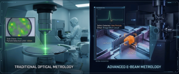
Traditional scanning surface inspection systems (SSIS) must now distinguish between intentional nanostructures and unwanted particulate matter at a scale where the two are nearly indistinguishable.
AI chips require massive dies with billions of interconnects. A defect that might have been tolerable in a mobile processor five years ago can now render an entire high-cost AI accelerator useless.

This shift has moved metrology from a quality check to the very foundation of the manufacturing process.
To calibrate the hyper-sensitive inspection tools used in today’s fabs, the industry has adopted new standards that provide absolute traceability and repeatable accuracy.
Calibration is only as good as the reference material. Modern metrology relies on NIST-traceable Polystyrene Latex (PSL) microspheres and Silica wafer standards.
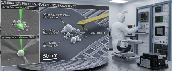
These standards allow engineers to verify that their inspection tools can accurately detect and size particles at the 10nm, 5nm, and even 3nm thresholds.
It is no longer enough to have the particles simply; they must be placed with extreme precision.
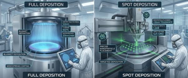
Full deposition and Spot deposition techniques are used to create calibration wafers that mimic real-world contamination scenarios.
While PSL has been the industry workhorse, 2026 has seen a significant shift toward Silica Nanoparticle Standards.
Silica provides a refractive index closer to that of the materials actually found in the fab, offering a more realistic calibration for the latest Deep Ultraviolet (DUV) and Extreme Ultraviolet (EUV) lithography inspection tools.
For a leading-edge fab, the difference between a 70% yield and an 85% yield represents billions of dollars in annual revenue. Next-gen metrology standards provide the data integrity needed.
As we look toward the end of 2026, the competitive landscape of semiconductor manufacturing will be defined by those who can master the invisible.
The integration of AI into the manufacturing process itself, using machine learning to analyze metrology data in real-time, only works if the underlying calibration data is flawless.

By utilizing advanced wafer standards and precision contamination control, manufacturers aren’t just following the roadmap; they are ensuring that the 1nm frontier is both reachable and profitable.
The shift to 1nm nodes necessitates a new era of metrology where NIST-traceable standards are the foundation of manufacturing success.
By prioritizing precision calibration, fabs can overcome the yield challenges of AI-centric fabrication and ensure long-term profitability.
These standards are the key to turning the invisible challenges of contamination into a measurable competitive advantage.
At the 1nm scale, even a 5nm particle can cause a killer defect. Since AI chips have billions of dense interconnects, extreme metrology precision is required to prevent these microscopic contaminants from ruining expensive wafers.
NIST-traceable standards provide a certified, globally recognized baseline for calibration. They allow engineers to verify that their inspection tools are accurately detecting and sizing particles at the sub-10nm level with total repeatability.
While PSL (Polystyrene Latex) is a classic standard, Silica nanoparticles have a refractive index much closer to the materials used in actual chip production. This makes Silica more effective for calibrating advanced EUV and DUV lithography tools.
Next-gen metrology directly increases wafer yields and reduces tool downtime. By identifying defects earlier and calibrating tools faster, manufacturers save billions of dollars and maintain a competitive edge in the high-stakes AI chip market.