In the world of semiconductor manufacturing and cleanroom validation, the margin for error is nonexistent.
As microchips become smaller and more complex, the ability to detect and quantify sub-micron particles on silicon wafers is critical.
This is where PSL (Polystyrene Latex) Spheres, the gold standard for metrology calibration, play a pivotal role.
Understanding the science behind these spheres is essential for any facility looking to improve the accuracy of its Scanning Surface Inspection Systems (SSIS).
Polystyrene Latex (PSL) spheres are uniform, spherical particles synthesized from polymer materials. In metrology, they are utilized as size standards because of their incredible dimensional stability and uniform shape.
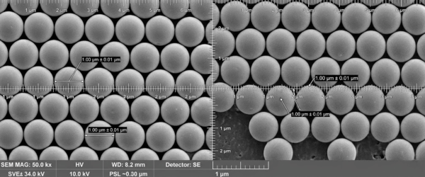
These spheres are typically suspended in deionized water and are engineered to have a near-perfect spherical geometry. Because their size can be measured with extreme precision using differential mobility analyzers or electron microscopy, they serve as the ruler for calibrating optical particle counters and wafer inspection tools.
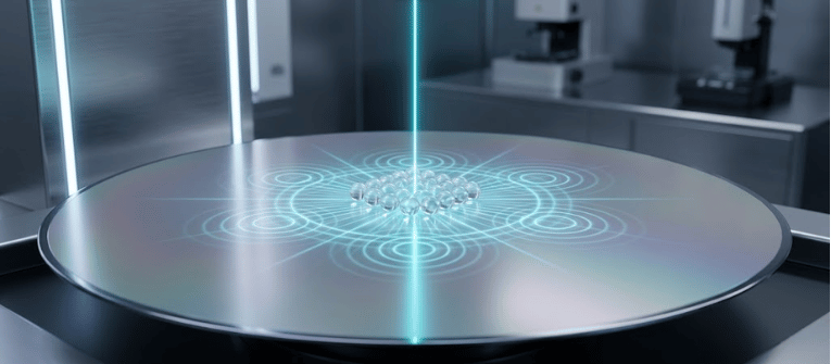
A Scanning Surface Inspection System (SSIS) uses laser light scattering to detect contamination on a wafer surface. However, a laser doesn’t inherently know the size of a particle; it only measures the intensity of the light reflected off it.
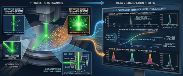
Without a known reference, the inspection tool cannot differentiate between a harmless artifact and a critical defect. PSL spheres provide this reference. By depositing a known size of PSL spheres onto a calibration wafer standard, engineers can program the SSIS to recognize specific light scattering intensities as specific particle sizes.
In high-stakes environments like semiconductor fabs, close enough isn’t an option. Calibration must be grounded in absolute truth.

NIST-traceable PSL spheres are particles whose size has been verified against the standards set by the National Institute of Standards and Technology.
Using NIST-traceable materials
In semiconductor fabrication, yield is the percentage of functional chips produced from a single wafer. Contamination is the leading cause of yield loss.
By using high-purity PSL spheres for routine calibration, facilities can fine-tune their SSIS sensitivity. This ensures that the equipment identifies real threats with high precision, directly protecting the bottom line and improving overall production efficiency.
| Parameter | Technical Specification / Value | Impact on SSIS Accuracy |
|---|---|---|
| Refractive Index ($n$) | 1.5905 @ 589 nm (25 °C) | Determines light scattering intensity used in Mie Theory calculations |
| Density ($\rho$) | 1.05 g/cm³ | Ensures neutral buoyancy in aqueous suspensions for uniform particle deposition |
| Material | Polystyrene / Divinylbenzene (DVB) | Provides high-dimensional stability and resistance to laser‑induced melting |
| Size Distribution (CV) | < 3% (Coefficient of Variation) | Guarantees monodispersity; essential for clear size‑peak identification |
| Surface Charge | Sulfate or Carboxyl Modified | Prevents particle clumping (agglomeration) during wafer deposition |
| Traceability | NIST (National Institute of Standards and Technology) | Provides a legal and technical benchmark for global quality audits |