

As the semiconductor industry aggressively scales toward 7nm, 5nm, and even smaller process nodes, the precision required for contamination monitoring has reached an inflection point.
For decades, Polystyrene Latex (PSL) microspheres have served as the industry gold standard for calibrating Scanning Surface Inspection Systems (SSIS).
However, as particle size detection requirements drop below the 20nm threshold, the physical limitations of PSL are becoming apparent, paving the way for the adoption of Silica Wafer Standards.
Silica (SiO2) microspheres offer a robust alternative that aligns more closely with the physical realities of modern semiconductor manufacturing.
Unlike PSL, Silica is an inorganic material with a high melting point and extreme structural rigidity.
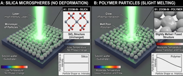
It can withstand the highest-intensity inspection lasers without deforming, ensuring the scattering signal remains constant across multiple calibration cycles.
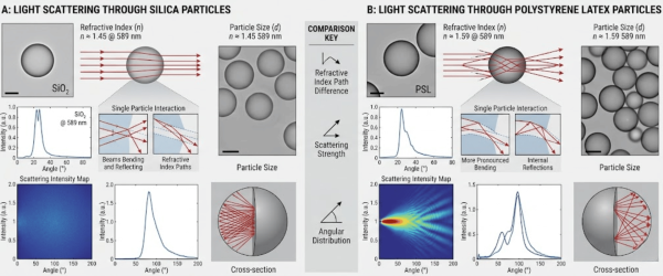
The refractive index of Silica is much closer to that of many actual cleanroom contaminants.
By using Silica Wafer Standards, metrology engineers can achieve a more realistic calibration of their SSIS tools, leading to higher capture rates for killer defects that might have been overlooked using traditional PSL calibration.
Silica particles do not shrink or outgas.
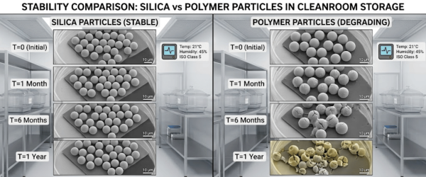
A Silica calibration wafer provides a more stable, long-term reference point, which is critical for maintaining tool-to-tool matching across a global fleet of inspection systems.
Polystyrene Latex spheres are soft, organic polymers. While they are highly uniform and easy to deposit, they present several challenges when used to calibrate tools for sub-20nm inspection.
High-intensity UV and EUV inspection lasers can melt or deform PSL spheres at smaller sizes.
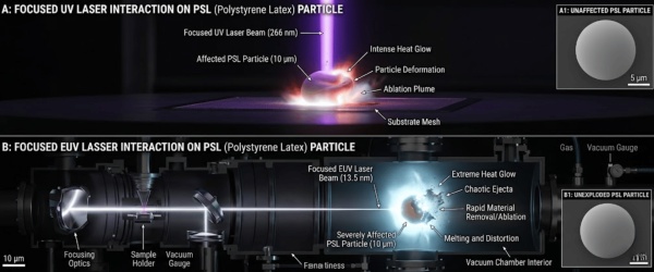
This deformation changes the scattering cross-section, leading to inaccurate tool calibration.
The refractive index of PSL differs significantly from the real-world contaminants (like silicon shards or metallic flakes) found in a vacuum-sealed fabrication environment.
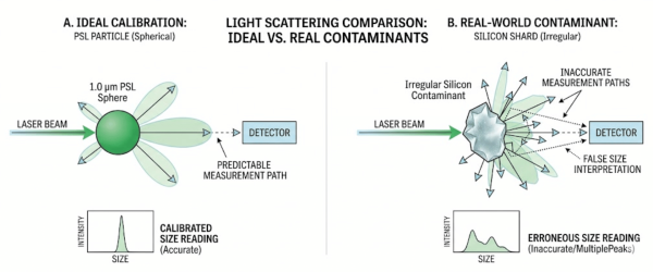
This mismatch can lead to a sizing error in which the tool incorrectly estimates the magnitude of a defect.
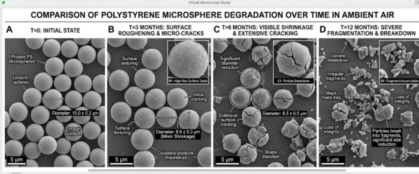
Organic PSL spheres are prone to shrinking or degradation when exposed to atmospheric conditions over long periods, reducing the shelf-life of the calibration standard.
| Technical Attribute | Polystyrene Latex (PSL) | Silica (SiO₂) Standards |
|---|---|---|
| Material Base | Organic polymer | Inorganic amorphous silica |
| Thermal Stability | Low (susceptible to laser damage) | High (laser resistant) |
| Refractive Index | ~1.59 (fixed) | ~1.46 (closer to real‑world contaminants) |
| Particle Rigidity | Soft (can deform under vacuum) | Hard (maintains spherical integrity) |
| Size Accuracy | Suitable for >32 nm nodes | Critical for sub‑20 nm nodes |
| Chemical Resistance | Low (reacts with cleanroom fluids) | High (inert to most chemicals) |
| Long‑term Stability | Prone to shrinkage and degradation | Exceptional shelf life and stability |
For any calibration standard to be valid in a high-volume manufacturing (HVM) environment, it must be NIST traceable. We utilize rigorous deposition techniques to ensure that Silica particles are distributed with high uniformity across the wafer surface.
Whether using Full Deposition for tool sensitivity testing or Spot Deposition for size calibration, the traceability to National Institute of Standards and Technology (NIST) protocols ensures that the metrology data collected in the fab is legally and technically defensible.
In the sub-20nm era, even a single 15nm particle can result in a catastrophic circuit failure. The shift from PSL to Silica is not merely a technical preference; it is a necessity for yield optimization.
While PSL remains a valuable tool for larger-node metrology and general aerosol testing, the industry’s move toward sub-20nm nodes demands the stability and accuracy of Silica.
By integrating Silica Wafer Standards into regular calibration cycles, semiconductor manufacturers can ensure their inspection systems are tuned to the highest possible fidelity, safeguarding yields and accelerating the path to market for next-generation silicon.
Silica is an inorganic material with a high melting point, making it resistant to laser damage from advanced inspection tools. Unlike PSL, it doesn’t deform or shrink, ensuring precise calibration at extremely small scales.
Yes. High-quality Silica standards are manufactured using NIST-traceable particles. This ensures that the size distributions and concentrations meet international metrology requirements for strict industry compliance.
By providing a more realistic refractive index and better thermal stability, Silica standards allow for more accurate tool calibration. This reduces false positives and ensures that killer defects are detected early in the process.