The semiconductor industry is rapidly advancing into sub-3nm nodes and the Angstrom era. As transistor sizes shrink, the margin for error in silicon wafer manufacturing has practically vanished.
In this high-stakes fabrication environment, a particle as small as 15 nanometers (nm) can disrupt an entire circuit, causing catastrophic yield loss.
To detect these microscopic threats, Scanning Surface Inspection Systems (SSIS) must operate with absolute precision. This precision is entirely dependent on sub-20nm calibration standards.
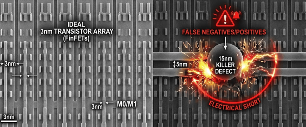
In traditional semiconductor nodes, particles under 20nm were considered negligible background noise. Today, they are classified as killer defects. When structural features on a chip are only a few nanometers wide, a 15nm particle acts like a boulder blocking a highway, causing short circuits or open circuits.
Standard inspection tools cannot reliably identify or size these micro-contaminants without exact calibration. If an SSIS tool is miscalibrated by even 1–2 nanometers, it will either miss critical defects entirely (false negatives) or flag harmless variations as threats (false positives), crippling factory throughput.
Most high-throughput wafer inspection tools rely on light-scattering technology. When a laser hits a particle on a wafer surface, the light scatters. The inspection tool measures this scattered light to determine the particle’s size and location.
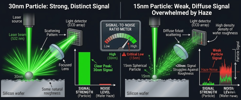
However, as particle sizes drop below 20nm, the physics changes drastically.
Without exact calibration using precise nanoparticles, inspection lasers cannot distinguish a true sub-20nm defect from background noise.
Achieving accurate calibration requires deposition standards with highly uniform particle sizes. Manufacturers primarily rely on two materials, each serving a specific role in high-precision metrology.
| Feature | Polystyrene Latex (PSL) Spheres | Silica Microspheres |
|---|---|---|
| Size Uniformity | Extremely high; monodisperse | High |
| Refractive Index | High, around 1.59; provides strong laser signals | Low, around 1.45; closely mimics real-world process particles |
| Material Stability | Vulnerable to degradation under high-intensity lasers | Highly stable under intense UV/DUV lasers |
| Primary Use Case | Baseline calibration of SSIS sizing accuracy | Real-world material simulation and laser tuning |
Investing in sub-20nm calibration isn’t just about laboratory precision; it is a critical business strategy that directly impacts profitability.
As the industry pushes the boundaries of physics, sub-20nm calibration standards remain the foundation of reliable, profitable, and flawless wafer inspection.
As the semiconductor industry pushes past traditional physical limits into the sub-3nm and Angstrom eras, managing microscopic contamination is no longer optional; it is a survival requirement for fabrication yields.
Sub-20nm calibration standards provide the foundational accuracy that Scanning Surface Inspection Systems (SSIS) need to isolate killer defects from background substrate noise.
By implementing a strict, monodisperse aerosol deposition protocol, manufacturers can confidently tune their laser metrology tools, eliminate costly false alarms, and safeguard their production profitability.
At advanced manufacturing nodes, transistor features are incredibly tiny. A particle as small as 15nm is large enough to bridge gaps between circuits, causing immediate short circuits or electrical failures that ruin the entire wafer yield.
The primary challenge is physics. Due to Rayleigh scattering, particles under 20nm scatter very little light. Laser scanners struggle to distinguish this weak signal from the natural surface roughness (haze) of the silicon wafer.
If the solution is too concentrated, multiple nanospheres will escape the atomizer nozzle inside a single water droplet. As the water evaporates, these spheres clump together, forming large doublets or triplets rather than a clean single-particle calibration standard.
Use PSL spheres for baseline sizing calibration because they offer extreme size uniformity and strong light scattering. Use Silica microspheres if you are using high-intensity UV/DUV lasers, as silica resists laser degradation better than plastic PSL.