

The semiconductor industry is currently navigating a transition where the margin for error has effectively vanished.
As fabrication facilities (fabs) move toward 3nm and 2nm process nodes, the killer defect is no longer a visible speck of dust; it is a microscopic particle often smaller than the wavelength of visible light.
In this environment, a single contaminant can render an entire wafer unusable, resulting in millions of dollars in lost yield.
To maintain profitability and performance, engineers must shift their focus from general cleanliness to high-precision metrology and calibration.
In previous decades, a 100-nanometer particle might have been an acceptable risk. Today, with Gate-All-Around (GAA) architectures and Extreme Ultraviolet (EUV) lithography, even a 10nm particle can cause a catastrophic short circuit or structural deformity in a transistor.
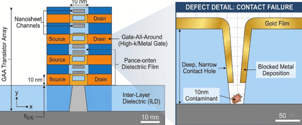
As chip features become smaller, the aspect ratio of the trenches and holes on a wafer increases. A tiny particle trapped at the bottom of a contact hole prevents proper metal deposition, creating an open circuit that is impossible to repair.
Contamination impacts the manufacturing cycle in three distinct ways:
During lithography, particles on the mask or the wafer surface reflect or absorb light, causing ghost images or missing features.

Particles landing on the wafer during Thin Film Deposition create bumps or voids.
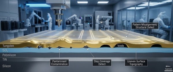
These irregularities prevent the next layer from lying flat, leading to a cumulative failure across multiple levels of the chip.
Not all contamination is physical.

Trace metallic particles can migrate through the silicon, altering the electrical properties of the transistor and causing latent failures, chips that work in the factory but fail after a month in the consumer’s hand.
To combat the threat of contamination, we provide the industry with the most reliable Contamination Wafer Standards.
These standards are used to calibrate KLA‑Tencor, Topcon, and Hitachi wafer inspection systems, ensuring that the exact size and density of particles present on the production line are accurately detected.
You cannot manage what you cannot measure. Scanning Surface Inspection Systems (SSIS) are the primary tools used to find these particles. However, these laser-based systems are only as accurate as the standards used to calibrate them.
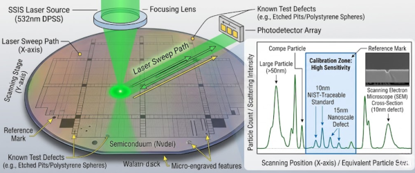
If an inspection tool is miscalibrated by even a few nanometers, it may miss a specific size of particle that is critical to the current process node. This is where high-precision wafer standards become the backbone of the production line.
Calibration is essential for the proper operation of inspection tools (SSIS). The table below clearly explains the technical differences between the various Applied Physics standards.
| Feature | PSL Wafer Standards | Silica Wafer Standards |
|---|---|---|
| Material | Polystyrene Latex Spheres | Silicon Dioxide (SiO₂) |
| Refractive Index | 1.59 @ 589 nm | 1.46 @ 589 nm |
| Durability | Low (sensitive to high laser power) | High (heat and laser resistant) |
| Node Application | General cleanroom testing | Advanced 5 nm, 3 nm nodes |
| Traceability | NIST traceable | NIST traceable |
| Deposition Type | Full or spot deposition | Full or spot deposition |
Compared to the past, chip features have now become so fine that even a 10 nm particle can destroy the structure of a transistor.

These particles deflect light during lithography, which leads to patterning errors. If they are not controlled in time, factory productivity declines and financial losses increase.
For manufacturers moving into the next generation of computing AI processors, 5G chipsets, and high-performance computing particle control is the primary differentiator between a profitable fab and a struggling one.

By utilizing Wafer Standards, metrology teams can ensure their inspection tools are operating at peak sensitivity. This allows for earlier detection of contamination sources, faster excursions (troubleshooting) when things go wrong, and ultimately, a much higher final yield.
To remain competitive in the 2nm and 3nm era, semiconductor manufacturers must treat particle contamination as their primary technical obstacle.
Reliable yield depends entirely on the precision of metrology tools, which can only be guaranteed through NIST-traceable calibration.
Utilizing high-performance wafer standards allows fabs to identify and eliminate defects before they impact the bottom line.
Ultimately, investing in accurate contamination control is the most direct path to achieving maximum profitability in advanced silicon fabrication.
Contamination typically originates from three areas: the mechanical wear of production equipment, chemical impurities in the processing gases, and the human operators themselves. Even in ultra-clean environments, microscopic skin flakes or hair can bypass filtration systems and land on the wafer surface.
NIST traceability ensures that the particles deposited on a calibration wafer are measured against a globally recognized legal standard. This chain of documentation gives engineers the certainty that their inspection tools are measuring particle sizes accurately according to international physics protocols.
PSL (Polystyrene Latex) spheres are standard for general sensitivity testing due to their uniform shape. However, Silica spheres are preferred for advanced nodes because they better mimic the refractive index of real-world contaminants and can withstand higher laser power during inspection without melting.
Spot deposition places particles in a specific, localized area on the wafer rather than across the entire surface. This allows engineers to map the exact sensitivity of the inspection tool’s sensors in a controlled environment, ensuring the machine detects defects consistently from the center to the edge.
Frequency depends on the production volume, but most high-yield fabs perform calibration checks daily or at the start of every new batch. Regular calibration prevents tool drift, where the machine’s accuracy slowly degrades over time, potentially leading to thousands of undetected defects.